Insulated gate field-effect transistor and its manufacturing method, and imaging device and its manufacturing method
- Summary
- Abstract
- Description
- Claims
- Application Information
AI Technical Summary
Benefits of technology
Problems solved by technology
Method used
Image
Examples
first embodiment
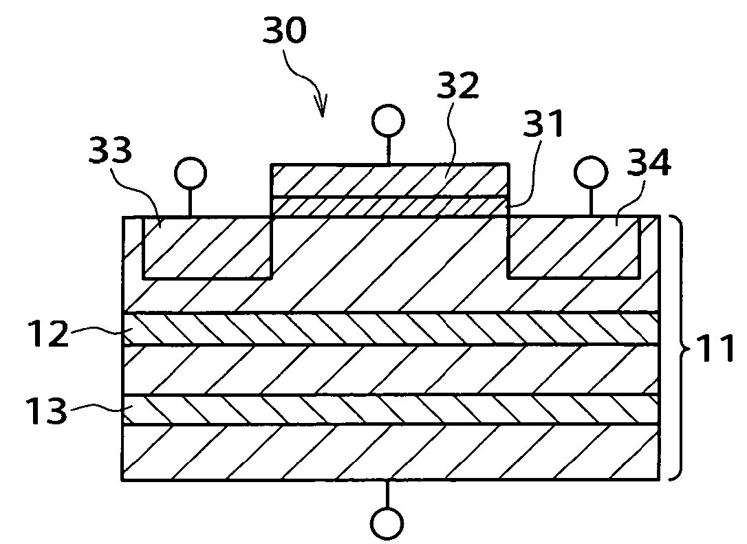
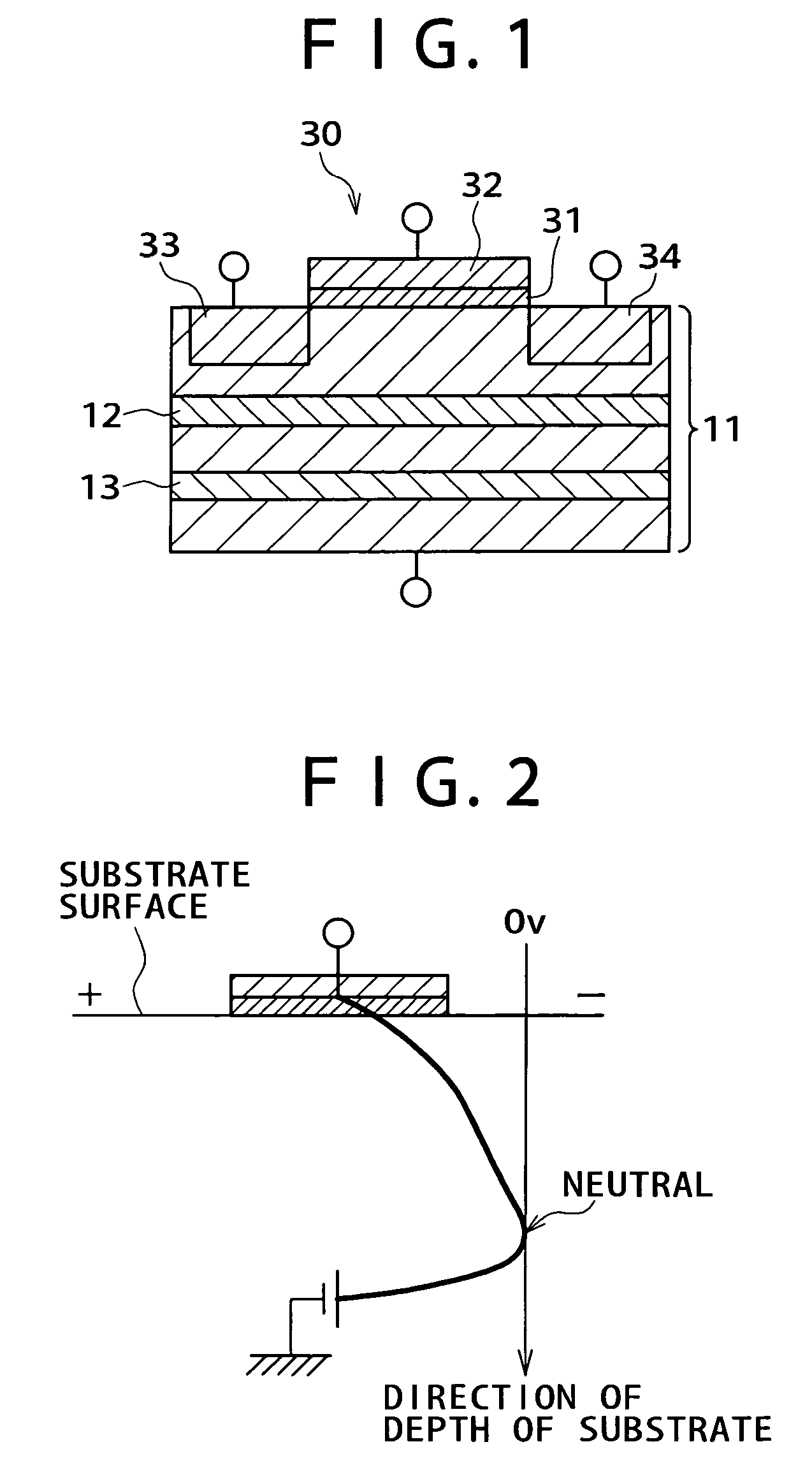
[0036] an insulated gate field effect transistor according to the present invention will be described with reference to a schematic structure sectional view of FIG. 1.
[0037] As shown in FIG. 1, a gate electrode 32 is formed on an N type semiconductor substrate 11 with a gate insulating film 31 interposed between the N type semiconductor substrate 11 and the gate electrode 32. A source region 33 and a drain region 34 of a P type are formed in the semiconductor substrate 11 on both sides of the gate electrode 32.
[0038] In addition, a P+ type first diffusion layer 12 is formed in the semiconductor substrate 11 at a position deeper than the source region 33 and the drain region 34. The first diffusion layer 12 has a peak position of impurity concentration at a depth of 0.6 μm or less from a surface of the semiconductor substrate 11, preferably at a depth of 0.15 μm or more and 0.45 μm or less. The impurity concentration of the first diffusion layer 12 is 1×10¹⁶ / cm3 or more and 6×10¹⁶ / c...
second embodiment
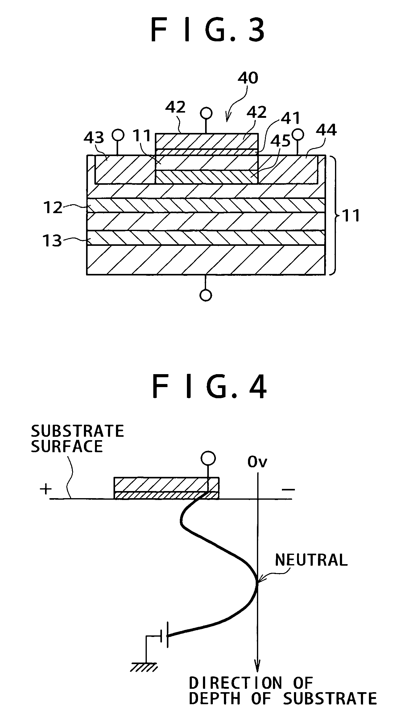
[0042] an insulated gate field effect transistor according to the present invention will next be described with reference to a schematic structure sectional view of FIG. 3.
[0043] As shown in FIG. 3, a gate electrode 42 is formed on an N type semiconductor substrate 11 with a gate insulating film 41 interposed between the N type semiconductor substrate 11 and the gate electrode 42. A source region 43 and a drain region 44 of a P type are formed in the semiconductor substrate 11 on both sides of the gate electrode 42. In addition, an N type diffusion layer 45 is formed between the source region 43 and the drain region 44 in the semiconductor substrate 11 with a region of the semiconductor substrate 11 left on the gate electrode 42 side.
[0044] Further, a P+ type first diffusion layer 12 is formed in the semiconductor substrate 11 at a position deeper than the source region 43 and the drain region 44. The first diffusion layer 12 has a peak position of impurity concentration at a depth...
PUM
 Abstract
Description
Claims
Application Information


