Solid-state imaging device, method for manufacturing the same and camera

Inactive Publication Date: 2005-12-08
PANASONIC CORP
View PDF5 Cites 14 Cited by
  • Summary
  • Abstract
  • Description
  • Claims
  • Application Information

AI Technical Summary

Benefits of technology

[0013] Therefore, with the foregoing in mind, it is an object of the present invention to provide a solid-state imaging device that has an on-chip filter capable of preventing color mixing from adjacent pixels due to angled light and can be made with a simpler manufacturing method.
[0016] With the present invention, it is possible to provide, at a lower cost, a solid-state imaging device that has an on-chip filter capable of preventing color mixing from adjacent pixels due to angled light.

Problems solved by technology

However, the light beams that are incident on the light receiving face of a color solid-state imaging element are not necessarily perpendicular to the light receiving surface and parallel to each other.
There is a problem in that color mixing occurs when light that is incident on the light receiving face from a direction that is inclined with respect to the light receiving face passes through a single color filter at an angle and is incident on an adjacent light receiving element.
However, in the conventional configuration noted above, there is the problem that a multitude of steps are necessary, ie.

Method used


Image

  • Solid-state imaging device, method for manufacturing the same and camera
  • Solid-state imaging device, method for manufacturing the same and camera
  • Solid-state imaging device, method for manufacturing the same and camera

Examples


embodiment 1

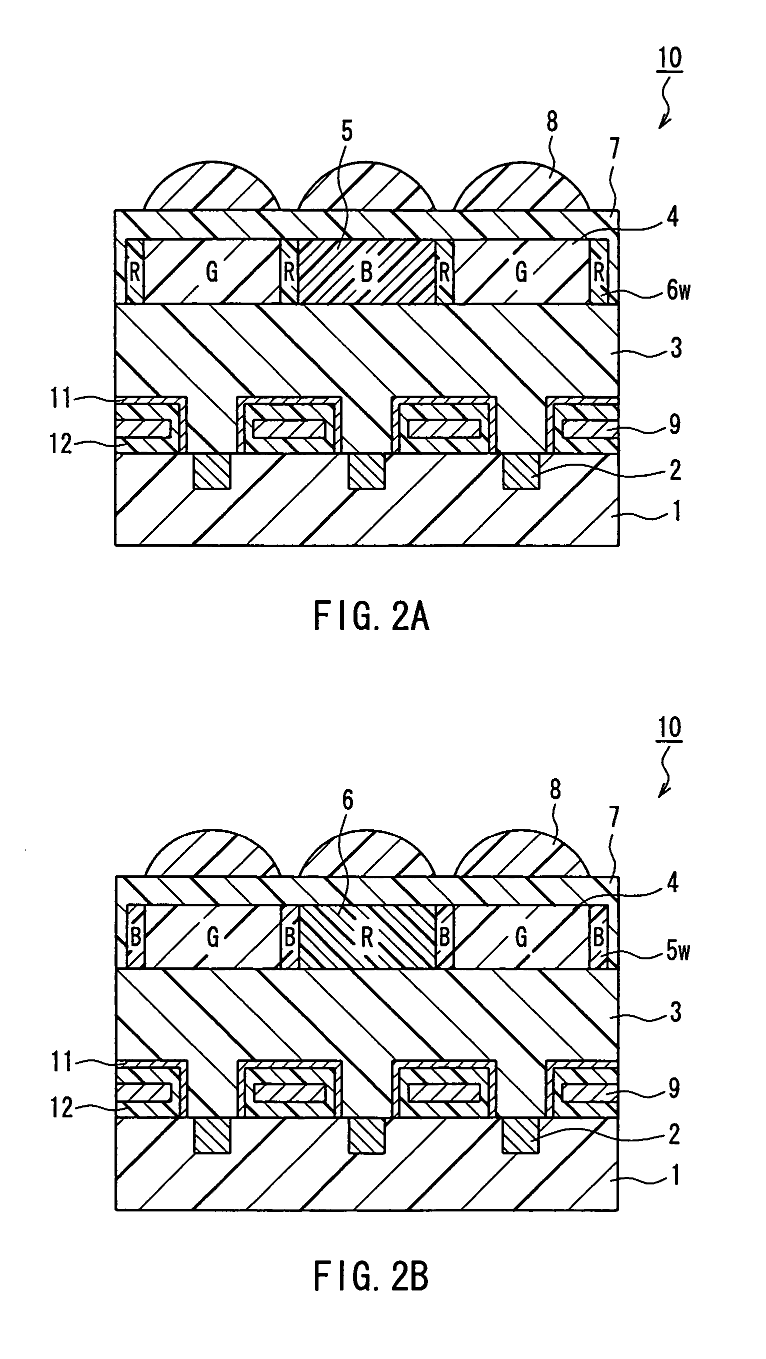
[0057] A solid-state imaging device according to one embodiment of the present invention is described below. It should be noted that a CCD solid-state imaging device is illustrated here as one embodiment, however the present invention is not limited to CCD solid-state imaging devices, and may also be applied to, for example, MOS solid-state imaging devices.

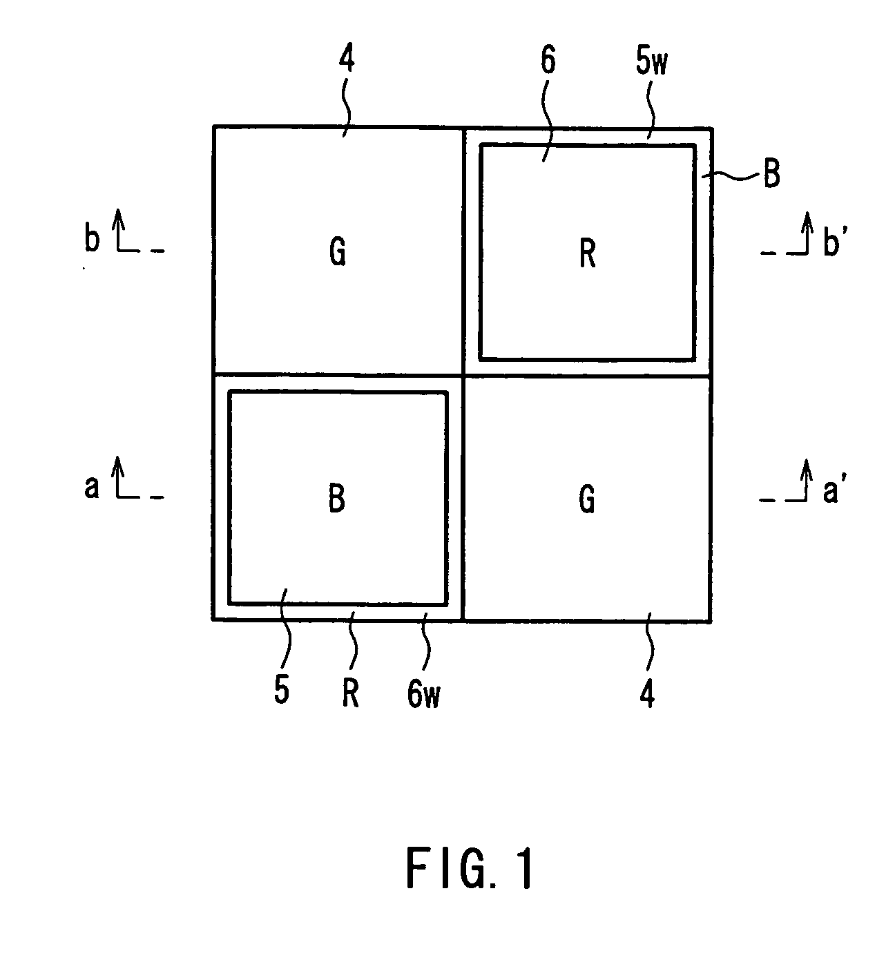
[0058] The solid-state imaging device according to the present embodiment has a color filter layer that is in what is known as a basic Bayer pattern, in which G color filters 4 are arranged on two diagonally opposite pixels of four 2 (h)×2 (w) pixels, wherein an R color filter 6 is arranged on one pixel of the remaining two pixels, and a B color filter 5 is arranged on the further remaining one pixel, such as shown in FIG. 1. However, there is a B color filter wall 5w on the border (pixel border region) of the G color filter 4 and the R color filter 6, and there is an R color filter wall 6w on the border (pixel border region) of ...

embodiment 2

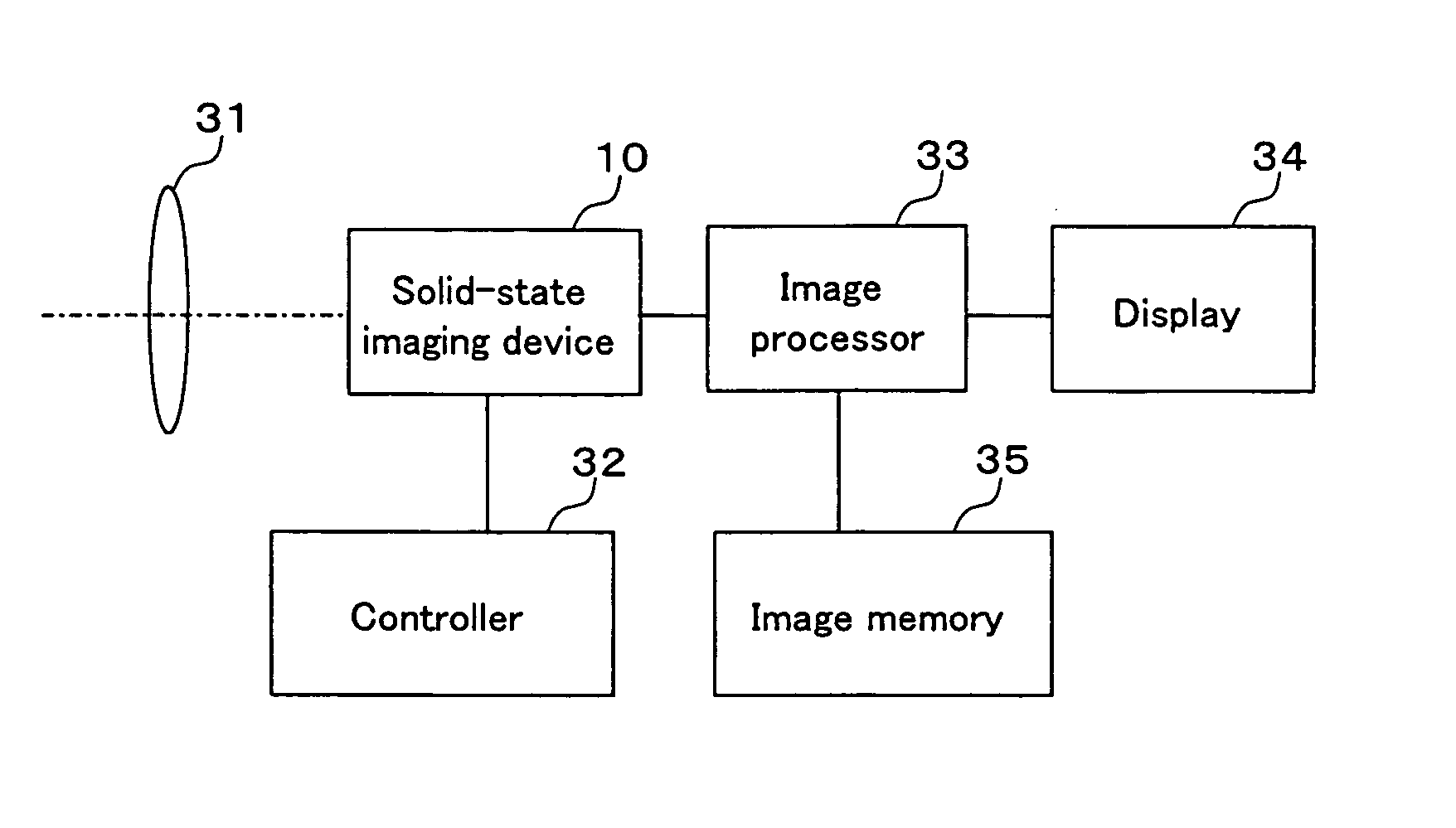
[0090] Another embodiment of the present invention is described with reference to FIG. 18.

[0091] If the solid-state imaging device described in Embodiment 1 is applied to a digital camera, then a digital camera that has superior picture quality due to prevention of color mixing can be realized at low cost. FIG. 18 is a block diagram showing a structural overview of the camera according to the present embodiment. As shown in FIG. 18, the camera according to the present embodiment is provided with, for example, a solid-state imaging element 10, an optical system 31 that includes lenses and the like for forming an image from the light that is incident from the object to be photographed on the imaging surface of the solid-state imaging device 10, a controller 32 for controlling the drive of the solid-state imaging device 10, an image processor 33 for processing various signals that are output from the solid-state imaging device 10, a display 34 for displaying the image signals that are...


PUM


Abstract

A solid-state imaging device that has an on-chip filter capable of preventing color mixing from adjacent pixels due to angled light is provided at low cost. The solid-state imaging device has light receiving elements formed in a matrix pattern on a semiconductor substrate and a color filter layer that is formed on the upper layer of the light receiving elements and is constituted by color filters of three or more colors. In the color filter layer, in at least a part of a pixel border portion in which color filters of two colors are adjacent, a color filter wall of a color that is different from the two colors is provided.

Description

BACKGROUND OF THE INVENTION [0001] 1. Field of the Invention [0002] The present invention relates to solid-state imaging devices that contain color on-chip filters, methods for manufacturing the same, and to cameras provided with the solid-state imaging devices. [0003] 2. Description of Related Art [0004] Conventionally, solid-state imaging devices such as CCD solid-state imaging devices that have photo-electric conversion portions for converting light to an electric charge, and MOS solid-state imaging devices have been used in various image input apparatuses such as video cameras and digital still cameras, or facsimiles. [0005] Color solid-state imaging devices that have color filters also are known as these solid-state imaging devices. Conventional color solid-state imaging devices have a configuration in which, for example, primary color filters made of a combination of red (R), blue (B) and green (G), or complementary color filters made of a combination of cyan (C), magenta (M),...

Claims


Application Information

Patent Timeline
IPC IPC(8): H01L31/0216H01L27/14H04N9/04H04N1/04H04N5/335H01L27/146H04N5/374H04N5/372H04N5/369H04N5/225
CPCH01L27/14621H01L27/14685H01L31/02162H04N5/2254H04N9/045H01L27/14627H04N25/136H04N25/134H01L27/148
Inventor KOBAYASHI, MASATO
Owner PANASONIC CORP
Why Eureka
Try Eureka