Module circuit board for semiconductor device having barriers to isolate I/O terminals from solder

Inactive Publication Date: 2005-12-15
LAPIS SEMICON CO LTD
View PDF13 Cites 7 Cited by
  • Summary
  • Abstract
  • Description
  • Claims
  • Application Information

AI Technical Summary

Problems solved by technology

In the solder reflow process, some problems occur.
If the solder ball reached the terminal is adhered to the terminal, the circuit board will be defective.
However, it is difficult to eliminate the formation of the solder ball comp

Method used


Image

  • Module circuit board for semiconductor device having barriers to isolate I/O terminals from solder
  • Module circuit board for semiconductor device having barriers to isolate I/O terminals from solder
  • Module circuit board for semiconductor device having barriers to isolate I/O terminals from solder

Examples


first embodiment

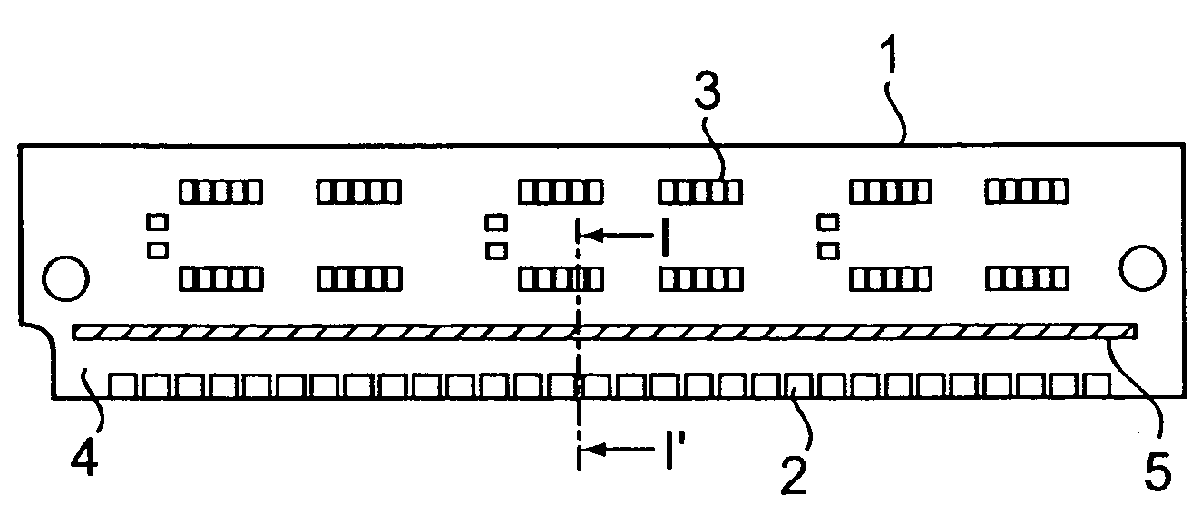
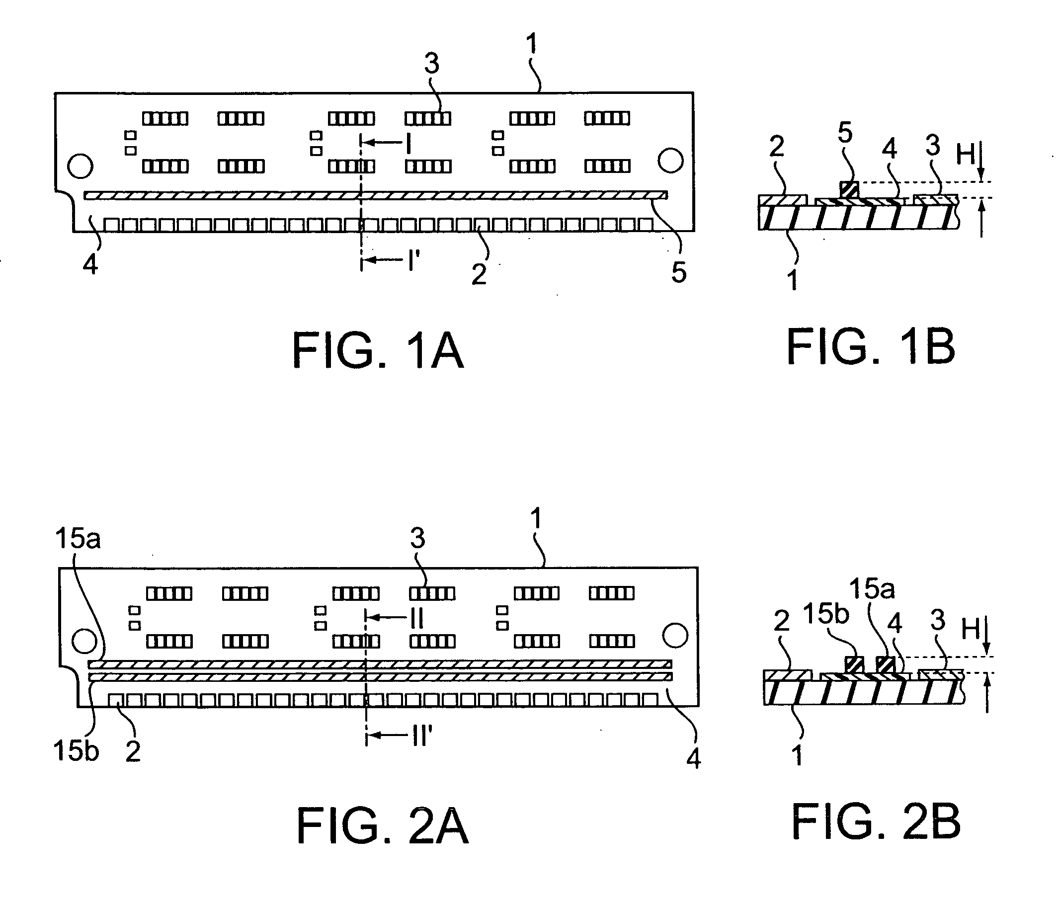
[0025] According to this first embodiment, if the solder ball is formed when the ICs are mounted on the board 1 during the solder reflow process, the solder ball can not get to the terminals 2 because the wall 5 acts as the barrier. Therefore, as it is not necessary to seal the terminals 2 with tape, process time can be reduced, and the tape adhesive does not remain on the terminals 2. As a result, the number of defective boards is dramatically decreased, and the uniform quality of the board can be achieved.

[0026] Referring to FIGS. 2(a) and 2(b), two walls 15a, 15b are formed on the resist film 4 between the terminals 2 and pads 3, along the terminals 2. The first wall 15a is disposed parallel to the second wall 15b. Each wall has a length of about 10 mm, so as to extend past the group of the terminals 2, and has a width of about 0.5 mm. The walls 15a, 15b act as barriers to isolate the terminals 2 form solder. The walls 15a, 15b are formed by the same method described in the first...

fifth embodiment

[0033] According to the invention, if the solder ball is formed when the ICs are mounted on the board 1 by the solder reflow process, the solder ball can not get to the terminals 2 because the solder ball will adhered to the metal pattern 46, which acts as the barrier. Further, as the metal pattern 46 is formed together with the other circuit pattern such as the power supply line 47, no additional processes to fabricate the board are necessary.

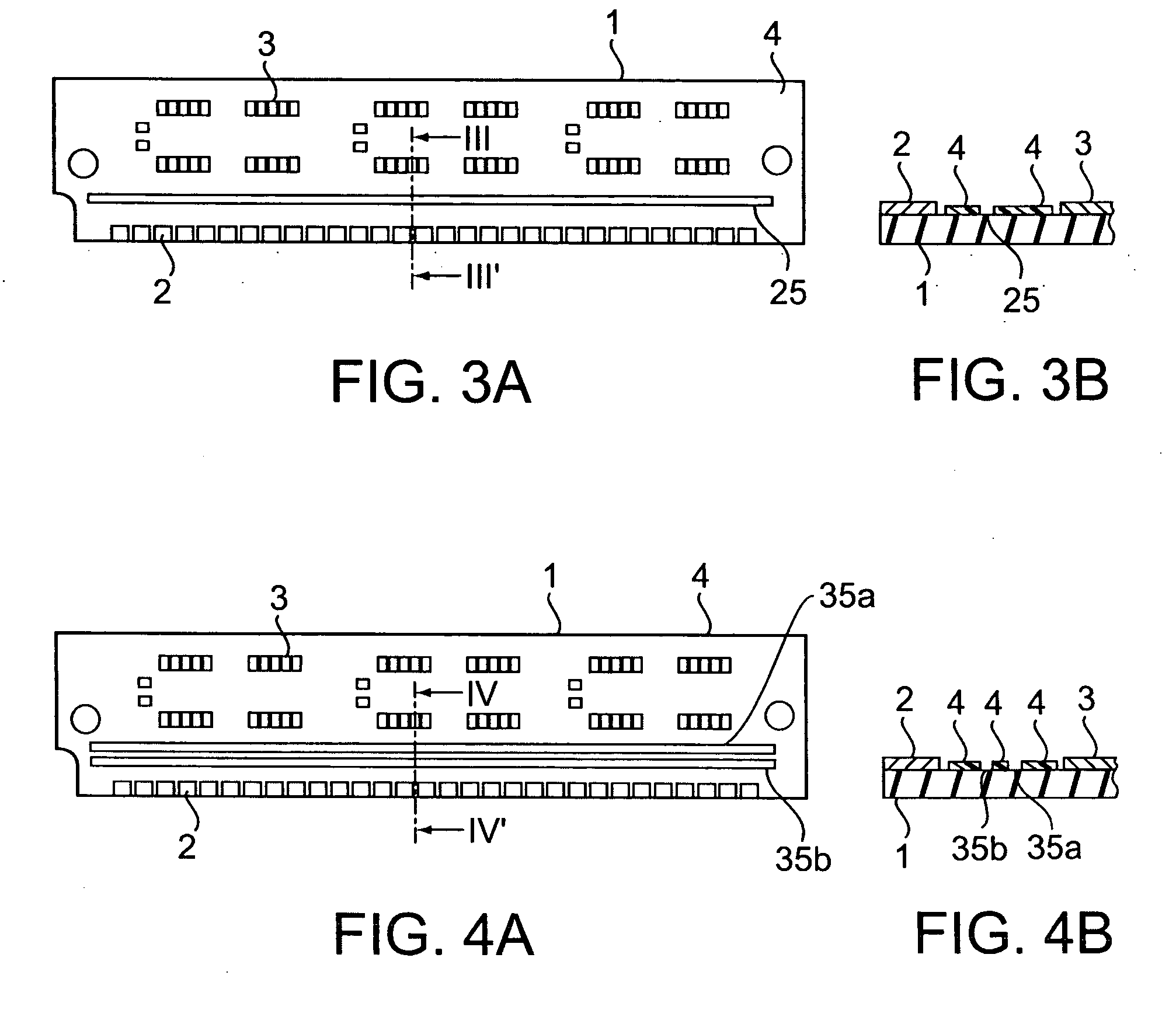
[0034] Referring to FIGS. 6(a) and 6(b), an elongated trench 55 is formed on the resist film 4 between the terminals 2 and pads 3, along the terminals 2. Furthermore, a wall 56, which is formed using the same method described in the first and second embodiments is formed on the resist film 4. The wall 56 is disposed between the trench 55 and terminals 2. The height h of the wall is not less than 0.1 mm, which is larger than a diameter of a solder ball which is formed during the solder reflow process. The surface of the board 1 is exposed at th...

sixth embodiment

[0035] According to the invention, if the solder ball is formed when the ICs are mounted on the board 1 using the solder reflow process, the solder ball can not get to the terminals 2 because the solder ball will be stacked in the trench 55. If the solder ball runs over the trench 55, the wall 56 as the second barrier dams the solder ball. If the distance between the trench 55 and the wall 56 is smaller than the diameter of the solder ball, the solder ball will be stacked between the trench 55 and the wall 56 strongly because of a surface tension effect of the solder ball.


PUM


Abstract

A module circuit board for a semiconductor device by a solder reflow process includes a plurality of pads on which the semiconductor device to be mounted, a plurality of terminals formed on a side edge of the board, a resist film covering an area between said pads and said terminal on the board, and a barrier formed between said pads and said terminals.

Description

CROSS-REFERENCE TO RELATED APPLICATION [0001] This application claims the priority benefit of Japanese Patent Application No. 10-354757, filed Dec. 14, 1998, the entire subject matter of which is incorporated herein of reference. BACKGROUND OF THE INVENTION [0002] 1. Field of the Invention [0003] The invention relates to a module circuit board including a plurality of I / O terminals disposed at an edge of the board, a plurality of soldering pads on its surface for mounting parts such as semiconductor devices, and a barrier formed on its surface to isolate the I / O terminals from solder. [0004] 2. Description of the Related Art [0005] A module circuit board for mounting flat type package ICs using a Surface-Mounted Device includes a plurality of I / O terminals plated of gold or flash gold which is formed on its one edge, a plurality of soldering pads on its surface on which the ICs are mounted using a solder reflow process, and a solder resist film formed on the circuit board. In the so...

Claims


Application Information

Patent Timeline
IPC IPC(8): H05K13/04H05K1/03H05K1/02H05K3/34H05K1/11
CPCH05K1/117H05K3/3452H05K13/0465H05K2201/0989H05K2201/09909H05K2203/0588
Inventor TAKAHASHI, NORIO
Owner LAPIS SEMICON CO LTD
Why Eureka
Try Eureka