Tape adhering method and tape adhering apparatus

a tape and tape technology, applied in the field of tape adhering methods, can solve the problems of low response of roller pressure to wafer, inability to easily determine the tension of the tape, and inability to easily adjust the pressure applied by the roller to the wafer, etc., to achieve the effect of reducing the amount of tape, and reducing the size of the formed semiconductor devi

Inactive Publication Date: 2005-12-22
TOKYO SEIMITSU
View PDF2 Cites 22 Cited by
  • Summary
  • Abstract
  • Description
  • Claims
  • Application Information

AI Technical Summary

Benefits of technology

[0024] Specifically, in the first aspect of the invention, the force exerted between the tape adhering means such as the roller and the wafer, via the tape, is obtained by moving only the movable table toward the tape adhering means. Therefore, the movement of the movable table does not interfere with the tension of the tape arranged above the movable table, and therefore the tape tension is not required to be taken into consideration when applying the force on the wafer by the movable table. As a result, the contact pressure applied on the wafer by the tape adhering apparatus can be accurately and quickly controlled to be uniform over the entire wafer. The contact pressure is defined as the pressure of the wafer per unit area.
[0071] Further, the tenth aspect of the invention may exhibit the effect that the pressure applied to the wafer can be controlled more accurately to be substantially equal over the whole wafer.

Problems solved by technology

This thickness difference remains as it is even after dicing, resulting in size variations in the formed semiconductor devices.
The tape characteristics such as the thickness, hardness and the bonding temperature are naturally varied from one tape to another, and therefore the tension of the tape cannot be easily determined.
Specifically, the tension of the tape contains the component opposite to the direction in which the force is applied to the wafer by the roller, and therefore, in the case where the roller is pressed against the wafer via the tape, the response of the pressure applied by the roller to the wafer become low, thereby making it difficult to perform a quick control operation.
Further, in view of the fact that the weight of the roller itself is imposed on the wafer, it is actually difficult to accurately control the force applied on the wafer by the roller.

Method used


Image

  • Tape adhering method and tape adhering apparatus
  • Tape adhering method and tape adhering apparatus
  • Tape adhering method and tape adhering apparatus

Examples


Embodiment Construction

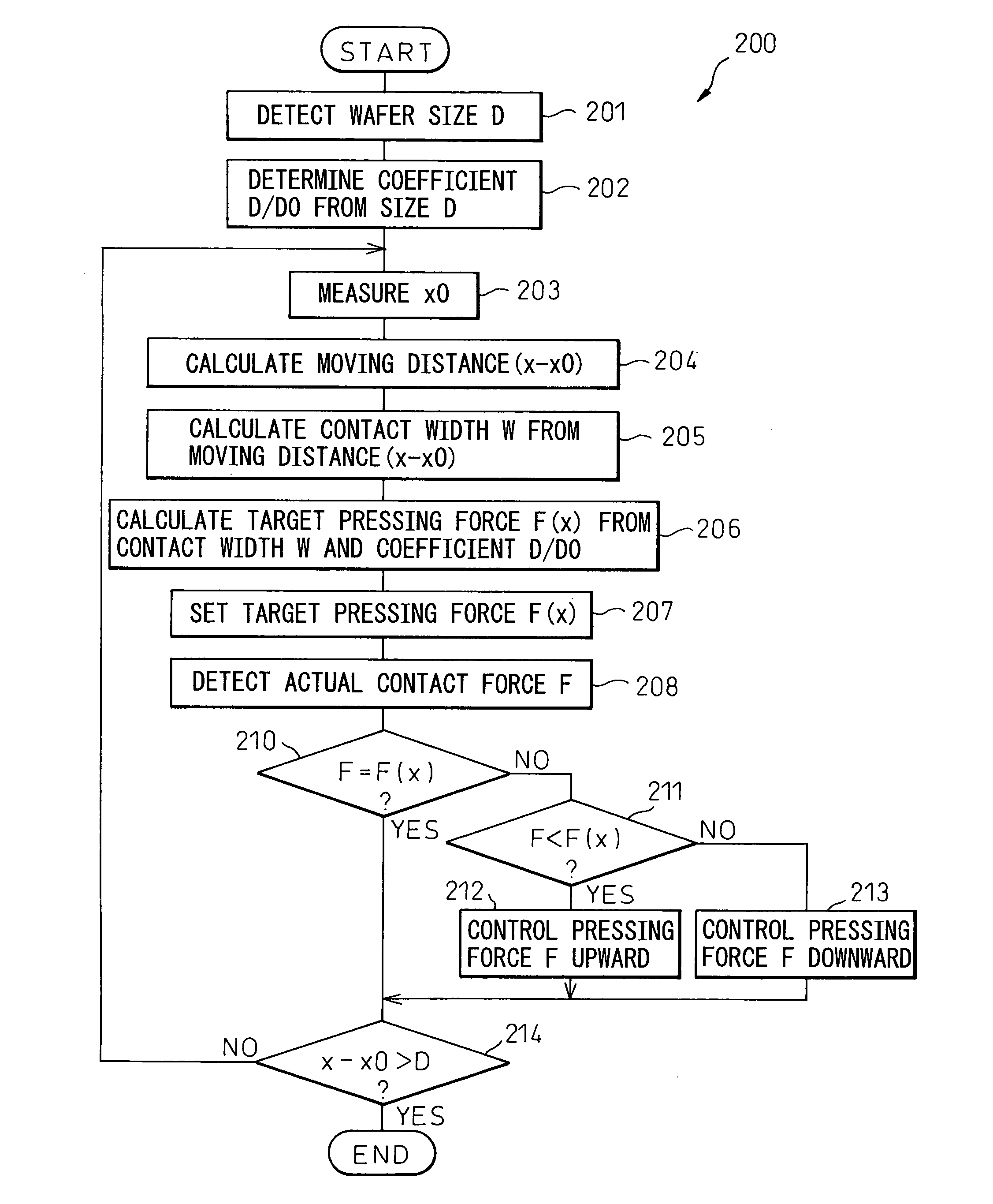
[0084] Embodiments of the invention are explained below with reference to the accompanying drawings. In the drawings, the same component parts are designated by the same reference numerals, respectively. For ease of understanding, these drawings are shown in different scales as required.

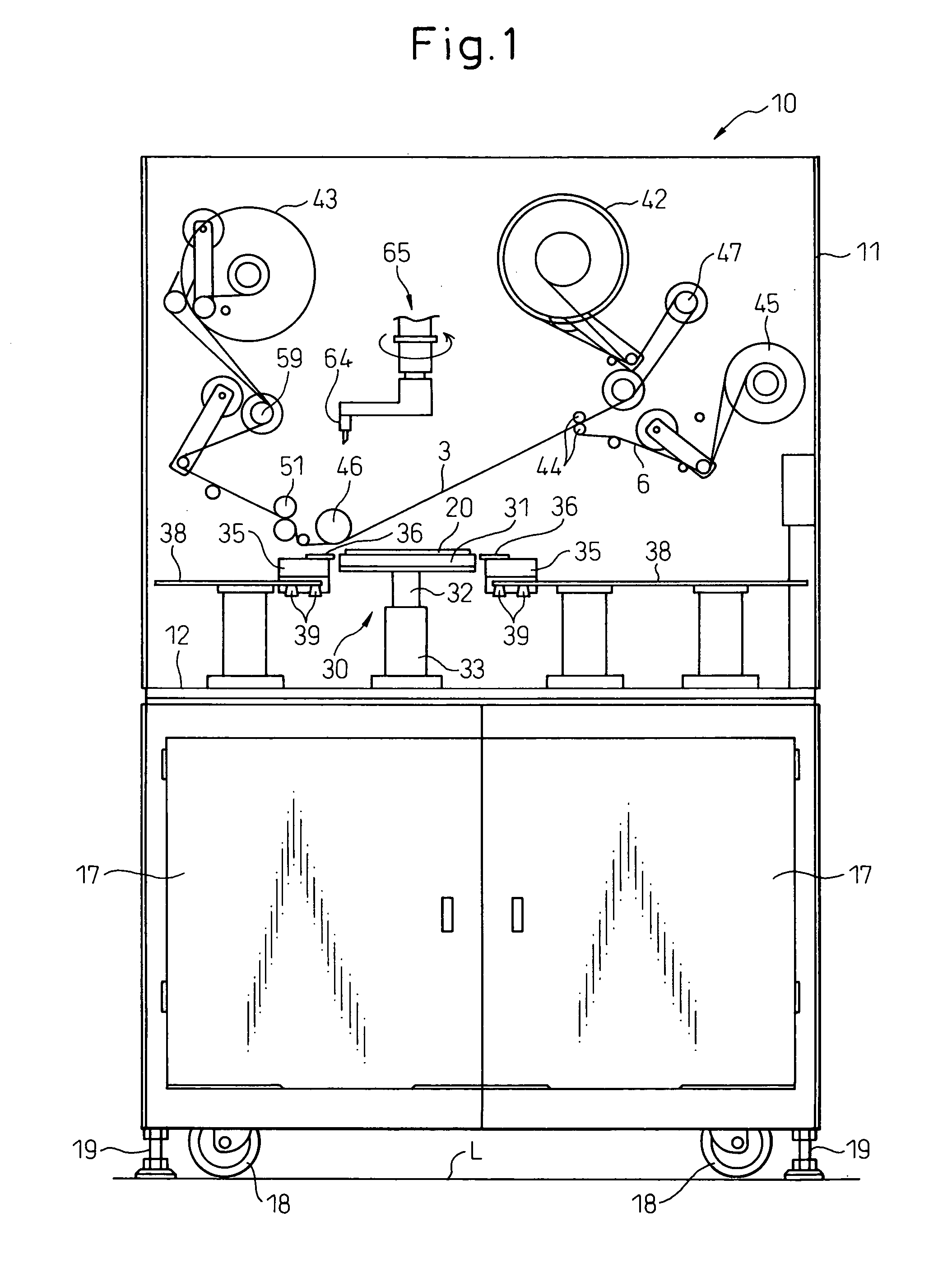
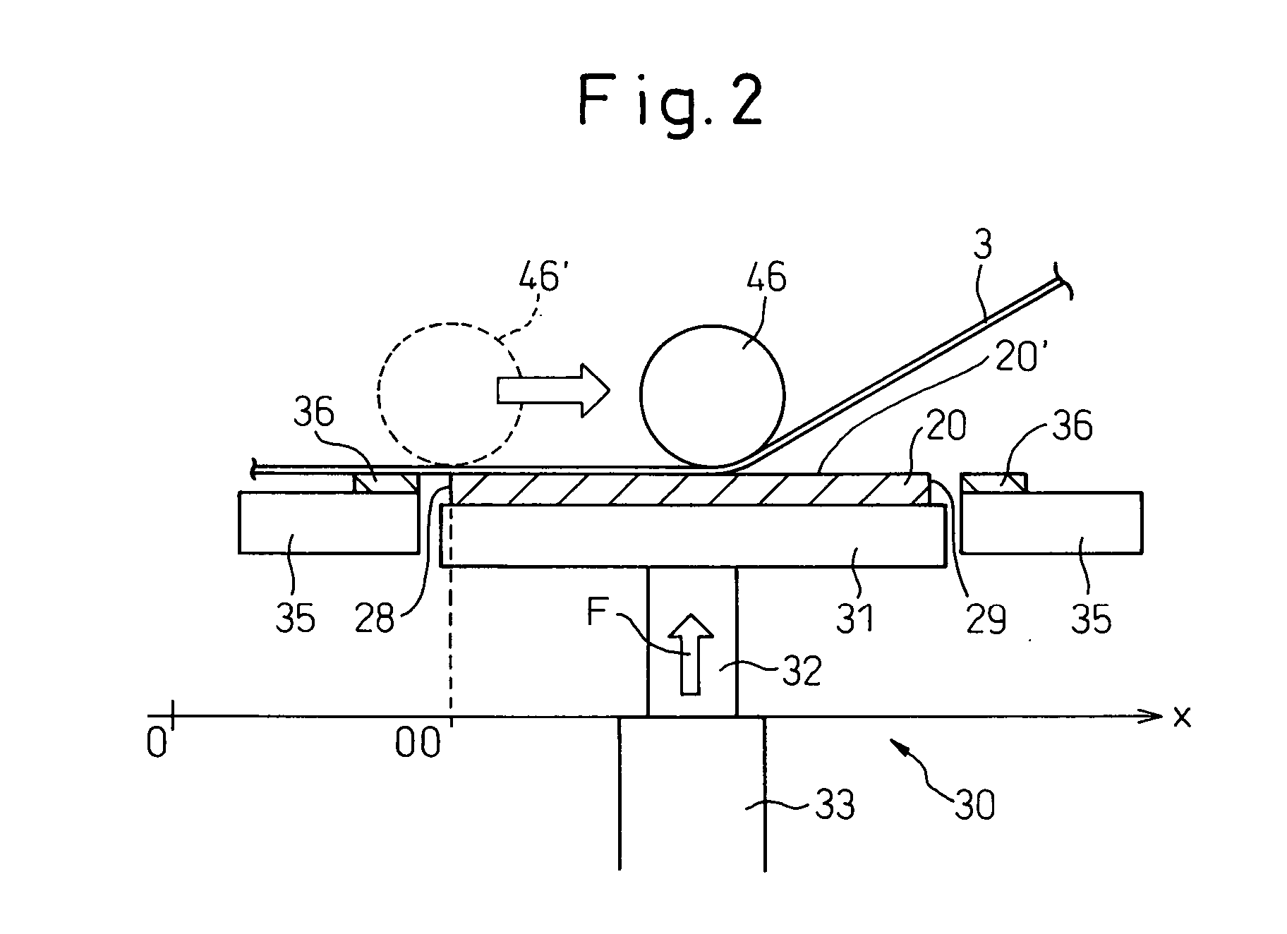
[0085]FIG. 1 is a sectional view schematically showing a tape adhering apparatus according to the invention. The tape adhering apparatus 10 shown in FIG. 1 comprises a housing 11 which contains a supply unit 42 for supplying a tape 3, for example a dicing tape or a surface protection tape to be adhered on a wafer 20, for example a silicon wafer, and a take-up unit 43 for taking up the tape from the supply unit 42. As shown in FIG. 1, a plurality of castors 18 and a plurality of stoppers 19 are arranged on the bottom surface of the housing 11. The tape adhering apparatus 10 can be moved to the desired position on the floor L by the castors 18, and fixed at the same position by the stoppers 19. A door...


PUM

PropertyMeasurementUnit
sizeaaaaaaaaaa
sizeaaaaaaaaaa
sizeaaaaaaaaaa

Abstract

A method and an apparatus for adhering a tape (3) on a wafer (20) are disclosed. The wafer is supported on a table (31), and the tape is supplied, between a tape adhering surface (20′) and a tape adhering unit (46), from a tape supply unit (42). The table is moved toward the tape adhering unit, whereby the tape adhering surface of the wafer on the table is pressed against the tape adhering unit through the tape with a force (F). Further, the tape adhering unit is moved from one end (28) to the other end (29) of the wafer in parallel to the tape adhering surface. The pressure (P) under which the tape adhering surface is in contact with the tape adhering unit through the tape is kept substantially uniform while the tape adhering unit moves from one end to the other end of the wafer. As a result, the pressure on the wafer is accurately equalized in spite of the movement of the tape adhering unit.

Description

BACKGROUND OF THE INVENTION [0001] 1. Field of the Invention [0002] The present invention relates to a tape adhering method, and to a tape adhering apparatus for carrying out the tape adhering method, which are used to adhere a tape such as a dicing tape on the back surface of a wafer or a surface protection tape on the front surface of the wafer. [0003] 2. Description of the Related Art [0004] In the field of semiconductor production, the trend is toward an ever-increasing size of the wafer. On the other hand, the wafer is becoming thinner and thinner to increase the density. In order to reduce the thickness of the wafer, the back surface of the semiconductor wafer is ground. In the process, a surface protection tape is adhered on the front surface of the wafer to protect the semiconductor elements formed on the front surface of the wafer. [0005] The wafer formed with semiconductor elements on the surface thereof is finally cut into cubes by a dicing machine. During the dicing proc...

Claims


Application Information

Patent Timeline
Patent Type & Authority Applications(United States)
IPC IPC(8): B65G49/07H01L21/00H01L21/301H01L21/46H01L21/78
CPCH01L21/67132H01L21/78
Inventor KOBAYASHI, KAZUOAMETANI, MINORU
Owner TOKYO SEIMITSU
Why Eureka
Try Eureka