Semiconductor device, manufacturing method of the semiconductor device, and design method of the semiconductor device

a semiconductor device and semiconductor technology, applied in the direction of cad circuit design, computer aided design, instruments, etc., can solve the problems of difficult fib processing, difficult to perform fib processing, and difficult to implement fib processing, so as to simplify the structure of the wiring cell

Inactive Publication Date: 2005-12-29
RICOH KK
View PDF7 Cites 8 Cited by
  • Summary
  • Abstract
  • Description
  • Claims
  • Application Information

AI Technical Summary

Benefits of technology

[0021] Another and more specific object of the present invention is to provide a semiconductor device, manufacturing method of the semiconductor device, and design method of the semiconductor device whereby wiring correction including cutting of a wiring can be easily performed.
[0076] According to this invention, it is possible to simplify a structure of the wiring cell.

Problems solved by technology

However, in a case where the correction is made by the FIB processing, in the semiconductor device having the multilayer wiring structure, other wiring is formed on the wiring that is a subject of the correction so that the wiring of the subject of the correction may be covered and therefore the FIB processing may be difficult.
Hence, it may be difficult to perform the FIB processing.
However, this Japanese Patent Application Publication does not disclose a detailed method for solving a problem where the wiring being a subject of the correction is covered with the upper layer wiring when the subject wiring is cut by the FIB processing so that it is difficult to implement the FIB processing.
Furthermore, a thickness sufficient for forming the dummy wiring is necessary so that the thickness of the semiconductor device may be large.
However, this Japanese Patent Application Publication does not disclose a detailed method for solving a problem where the wiring being a subject of the correction is covered with the upper layer wiring when the subject wiring is cut by the FIB processing so that it is difficult to implement the FIB processing.

Method used


Image

  • Semiconductor device, manufacturing method of the semiconductor device, and design method of the semiconductor device
  • Semiconductor device, manufacturing method of the semiconductor device, and design method of the semiconductor device
  • Semiconductor device, manufacturing method of the semiconductor device, and design method of the semiconductor device

Examples


first embodiment

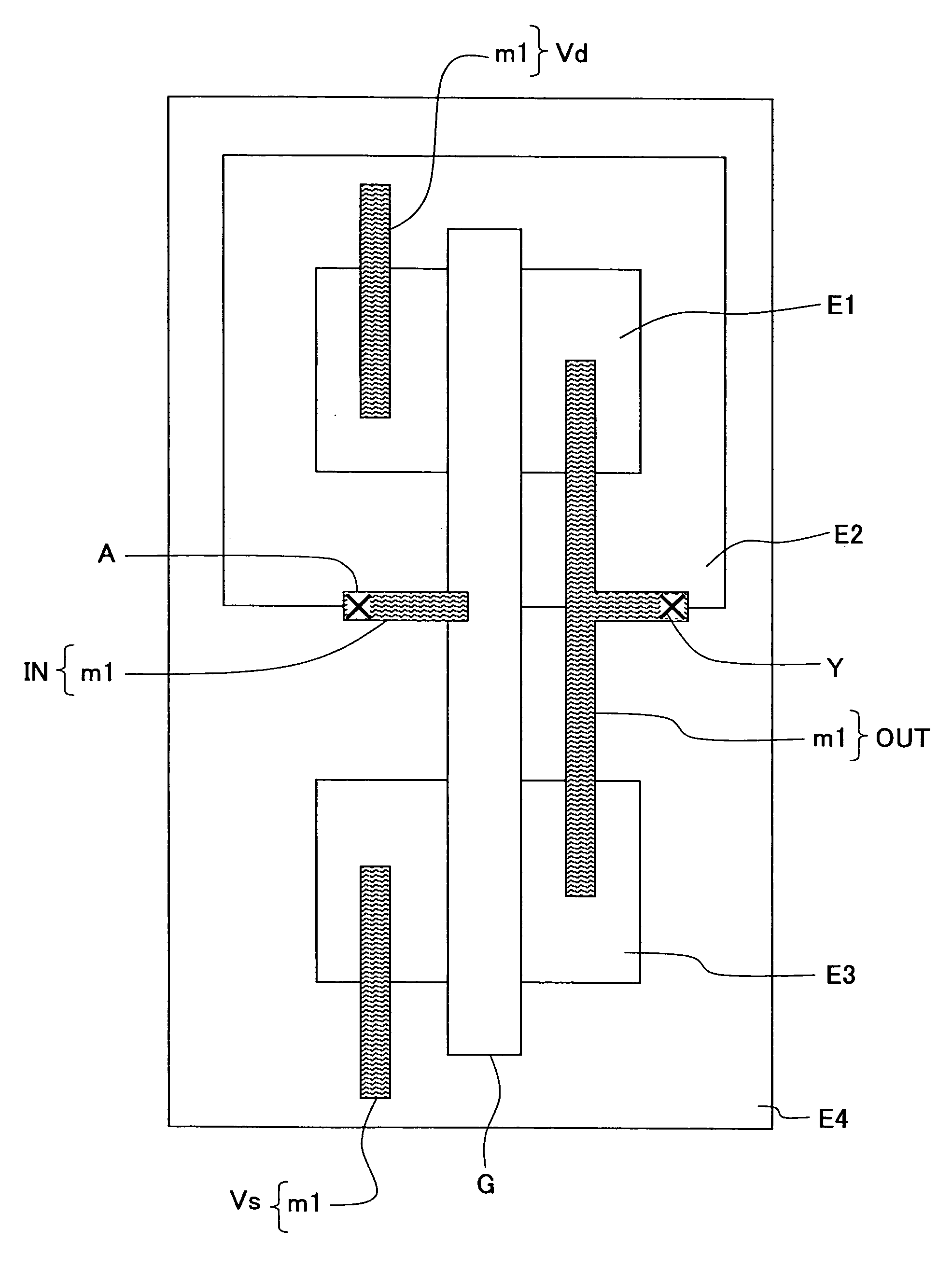
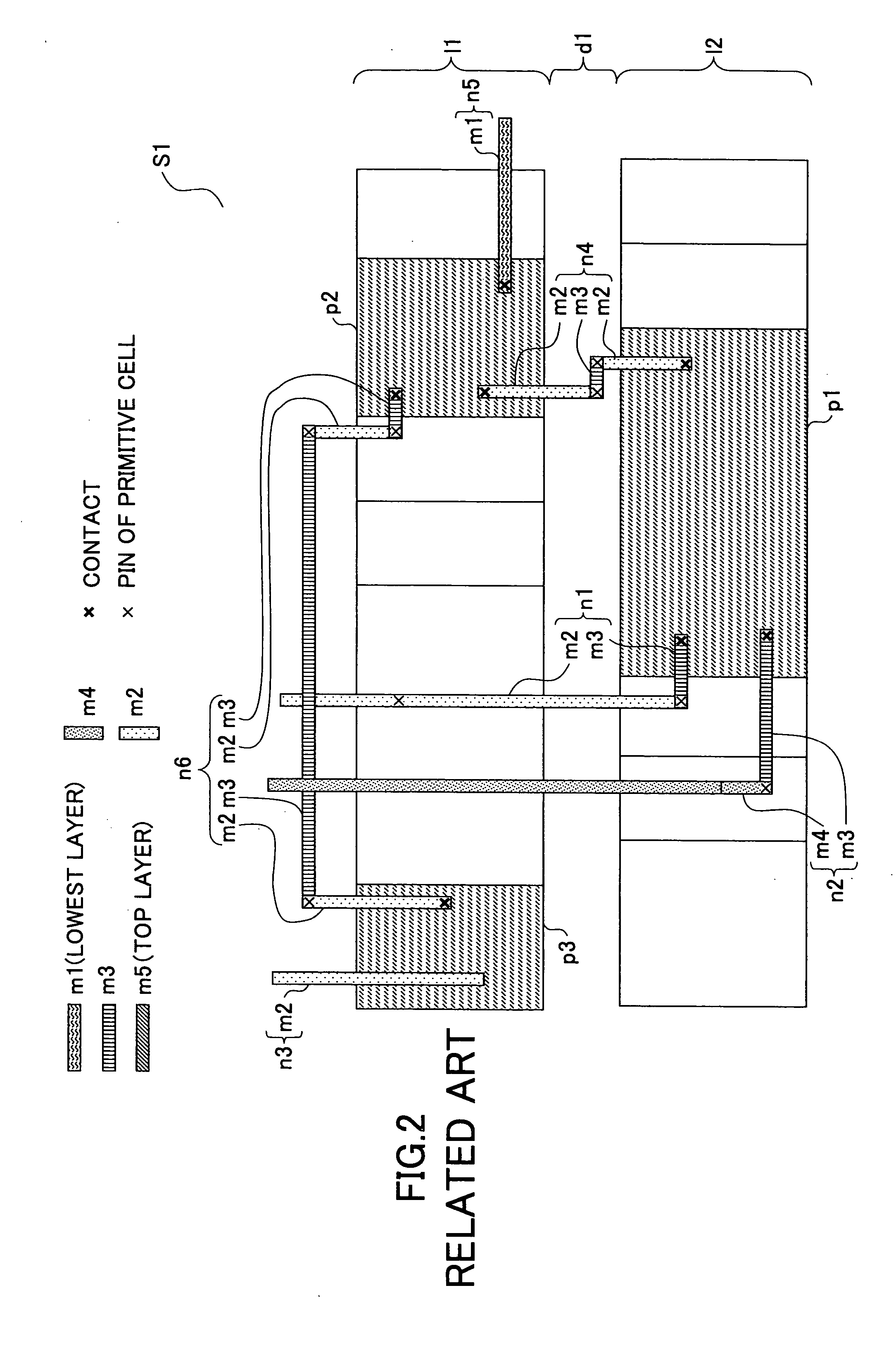
[0095] A semiconductor device in this embodiment has a multilayer wiring structure. Plural wiring layers, having plural wirings formed in a plane surface situated substantially parallel with a substrate surface where the device is formed are stacked. In the followings, the wiring layer formed in a side nearest to the substrate is described as a lowest layer wiring. The wiring layer formed at the top of the wiring layers stacked on the lowest layer wiring is described as a top layer wiring. For example, the top layer wiring may be covered with a protection layer (passivation layer).

[0096]FIG. 5 is a flowchart showing a manufacturing method of the semiconductor device of a first embodiment of the present invention.

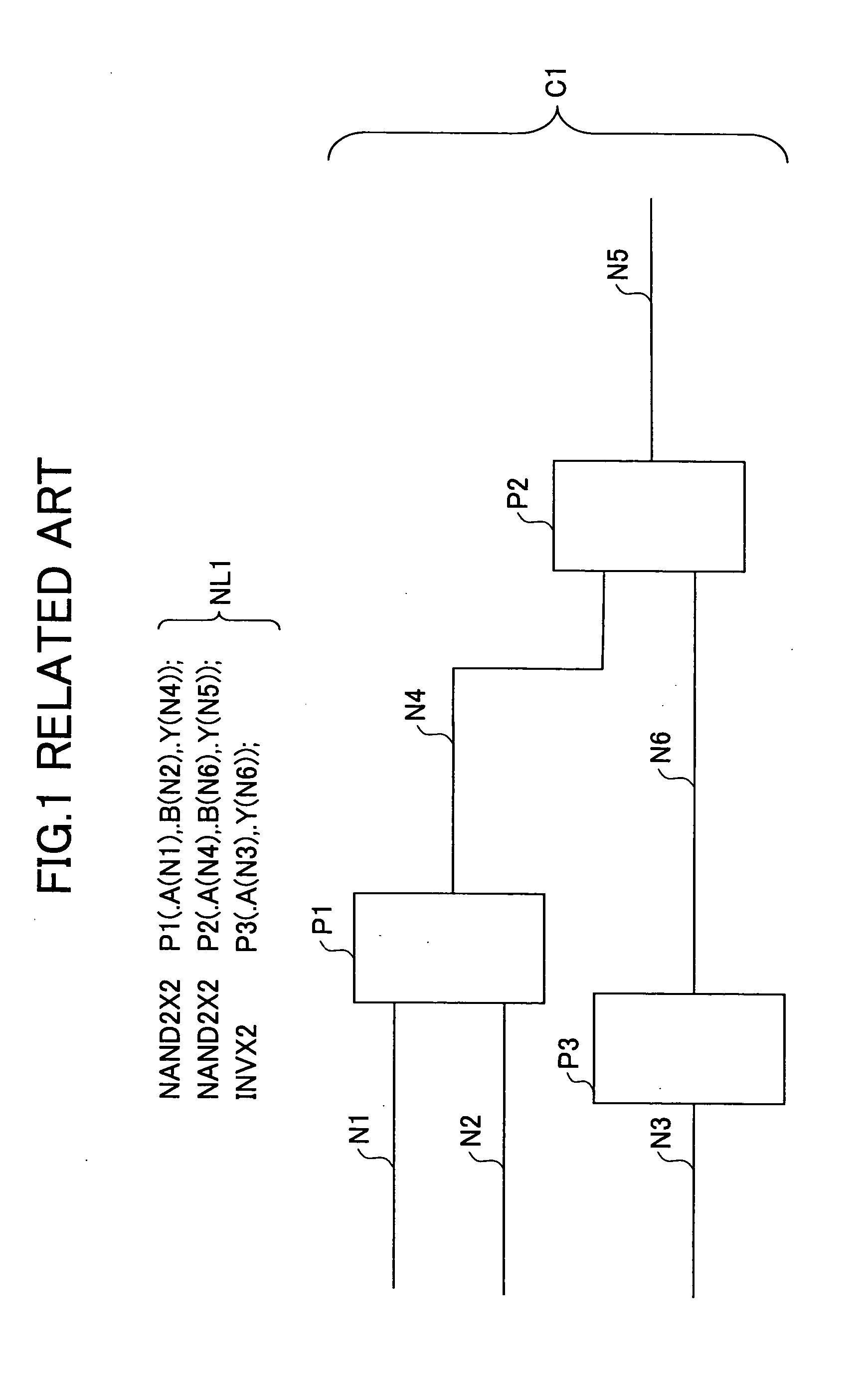
[0097] Referring to FIG. 5, in step 101, an arrangement of primitive cells wherein a circuit is defined and a connection circuit connecting the primitive cells is designed by using the automatic arrangement wiring tool. Based on the design, the primitive cells are arranged...


PUM


Abstract

A semiconductor device includes a plurality of primitive cells having multilayer wiring structures and formed on a substrate. The primitive cell includes a functional cell having a logic circuit and a wiring cell. The wiring cell includes a wiring part electrically connecting a plurality of the functional cells. The wiring part is a top layer connection wiring formed by a top layer wiring of the multilayer wiring structure.

Description

BACKGROUND OF THE INVENTION [0001] 1. Field of the Invention [0002] The present invention relates to semiconductor devices, manufacturing methods of semiconductor devices, and design methods of semiconductor devices, and more specifically, to a semiconductor device having a multilayer wiring structure, a manufacturing method of the semiconductor device, and a design method of the semiconductor device. [0003] 2. Description of the Related Art [0004] A circuit design support tool of a semiconductor device such as an automatic arrangement wiring tool may be used for forming an integrated circuit of the semiconductor device. By the automatic arrangement wiring tool, an arrangement of a primitive cell (“cell” or “standard cell”) which is a minimum unit circuit of a semiconductor integrated circuit is determined on a substrate, and a connection circuit connecting the primitive cells is designed and determined based on a net list where signal connection information between the primitive ce...

Claims


Application Information

Patent Timeline
Patent Type & Authority Applications(United States)
IPC IPC(8): G06F17/50H01L21/768H01L27/02H01L27/10H01L27/118H01L29/739
CPCG06F17/5068H01L27/11803H01L27/0203H01L21/76892G06F30/39
Inventor IWASAKI, MITSUTAKA
Owner RICOH KK
Why Eureka
Try Eureka