Decoupling capacitor for high frequency noise immunity

a capacitor and noise immunity technology, applied in capacitors, diodes, semiconductor devices, etc., can solve the problems of adding direct consumption of silicon area by the mis capacitor, processing steps, etc., and achieves the effect of reducing processing steps, reducing mask level and processing cost, and large capacitor fabrication area

Inactive Publication Date: 2006-01-12
MICRON TECH INC
View PDF23 Cites 1 Cited by
  • Summary
  • Abstract
  • Description
  • Claims
  • Application Information

AI Technical Summary

Benefits of technology

[0015] One capacitor embodiment includes a MIS (metal-insulator-silicon) capacitor fabricated on a silicon substrate, and another capacitor embodiment includes a MIM (metal-insulator-metal) capacitor fabricated at lower temperature between the interconnect layers above a silicon substrate. The MIS capacitor directly consumes the silicon area for fabrication of the capacitors, but potentially requires less processing steps when appropriately integrated with the gate insulator processing. The MIM capacitor does not directly impact silicon area and potentially provides a large area for capacitor fabrication. However, the MIM capacitor potentially impacts the number of required interconnect layers which adds mask level and processing cost.

Problems solved by technology

The MIS capacitor directly consumes the silicon area for fabrication of the capacitors, but potentially requires less processing steps when appropriately integrated with the gate insulator processing.
However, the MIM capacitor potentially impacts the number of required interconnect layers which adds mask level and processing cost.

Method used


Image

  • Decoupling capacitor for high frequency noise immunity
  • Decoupling capacitor for high frequency noise immunity
  • Decoupling capacitor for high frequency noise immunity

Examples


Embodiment Construction

[0034] The following detailed description of the invention refers to the accompanying drawings which show, by way of illustration, specific aspects and embodiments in which the invention may be practiced. In the drawings, like numerals describe substantially similar components throughout the several views. These embodiments are described in sufficient detail to enable those skilled in the art to practice the invention. Other embodiments may be utilized and structural, logical, and electrical changes may be made without departing from the scope of the present invention. The following detailed description is, therefore, not to be taken in a limiting sense, and the scope of the present invention is defined only by the appended claims, along with the full scope of equivalents to which such claims are entitled.

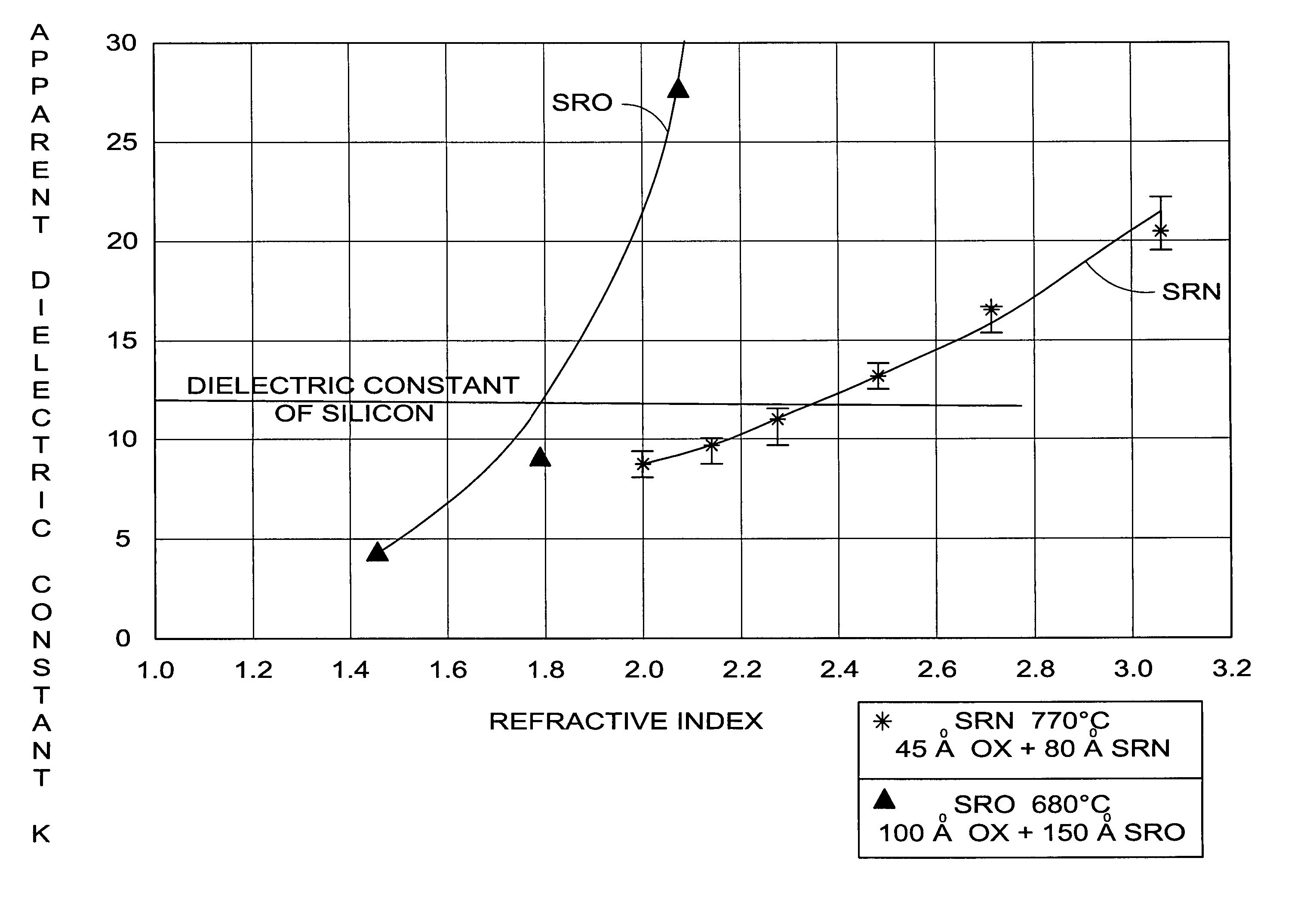
[0035] Silicon-rich nitride (SRN), or more particularly, injector SRN was referenced in the Background of the Invention. SRN is a subset of silicon rich insulator (SRI). Another s...


PUM

PropertyMeasurementUnit
frequenciesaaaaaaaaaa
dielectric constantaaaaaaaaaa

Abstract

Systems and methods are provided for an on-chip decoupling device and method. One aspect of the present subject matter is a capacitor. One embodiment of the capacitor includes a substrate, a high K dielectric layer doped with nano crystals disposed on the substrate, and a top plate layer disposed on the high K dielectric layer. According to one embodiment, the high K dielectric layer includes Al2O3. According to other embodiments, the nano crystals include gold nano crystals and gold nano crystals. One capacitor embodiment includes a MIS (metal-insulator-silicon) capacitor fabricated on silicon substrate, and another capacitor embodiment includes a MIM (metal-insulator-metal) capacitor fabricated between the interconnect layers above silicon substrate. The structure of the capacitor is useful for reducing a resonance impedance and a resonance frequency for an integrated circuit chip. Other aspects are provided herein.

Description

RELATED APPLICATION(S) [0001] This application is a divisional of U.S. patent application Ser. No. 10 / 752,351, filed Jan. 6, 2004; which is a divisional of U.S. patent application Ser. No. 09 / 944,986 filed on Aug. 30, 2001; each of which is incorporated herein by reference.TECHNICAL FIELD OF THE INVENTION [0002] This invention relates generally to integrated circuits and, more particularly, to decoupling capacitors for reducing resonance frequency and impendence in high-frequency chip designs. BACKGROUND OF THE INVENTION [0003] Goals for integrated circuit design include progressively scaling the design to achieve smaller feature sizes, and using faster clock frequencies beyond 1 GHz. Problems encountered in achieving these goals include the increasing voltage droop and the inductive noise of the active switching nodes, and further include the increasing power supply oscillations and the resulting noise that is generated and transmitted across the chip. [0004] These problems are add...

Claims


Application Information

Patent Timeline
Patent Type & Authority Applications(United States)
IPC IPC(8): H01L21/8242H01L21/02H01L21/28H01L21/3115H01L21/314H01L21/316H01L29/51H01L29/94
CPCB82Y10/00H01L21/28194H01L21/3115H01L21/3143H01L21/3162H01L27/0811H01L29/94H01L28/56H01L28/75H01L29/513H01L29/517H01L29/518H01L29/78H01L28/55H01L21/02271H01L21/0228H01L21/02183H01L21/02186H01L21/02266H01L21/02192H01L21/02197H01L21/02189H01L21/02274H01L21/02178
Inventor BHATTACHARYYA, ARUP
Owner MICRON TECH INC
Why Eureka
Try Eureka