

A Recessed Polysilicon Gate Structure for a Strained Silicon MOSFET Device
a technology of strained silicon mosfet and polysilicon, which is applied in the direction of semiconductor devices, electrical equipment, basic electric elements, etc., can solve the problems of gate leakage or shortening of the substrate, and achieve the effect of reducing the risk of shortening
- Summary
- Abstract
- Description
- Claims
- Application Information
AI Technical Summary
Benefits of technology
Problems solved by technology
Method used
Image

Examples
Embodiment Construction
Background of Invention
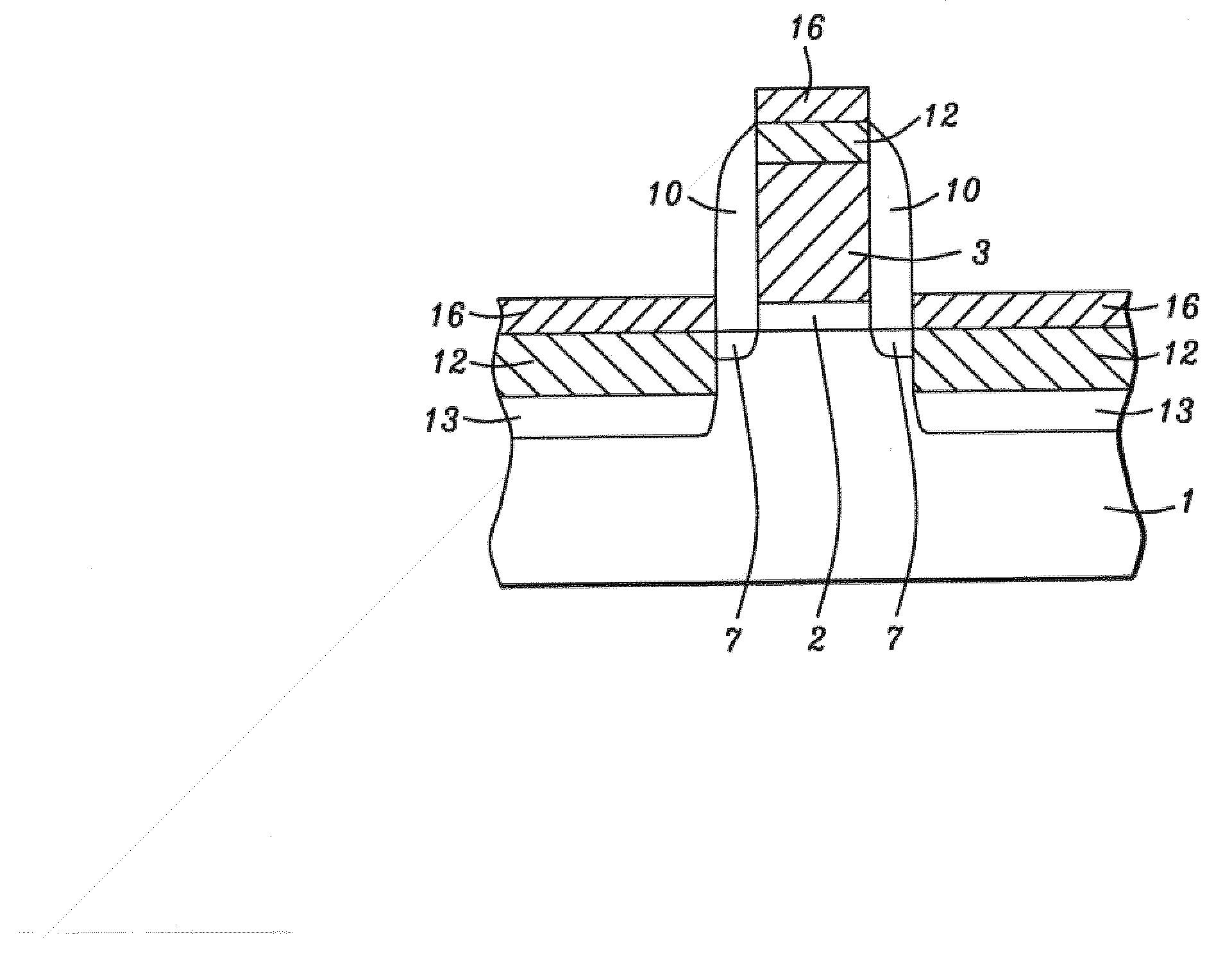
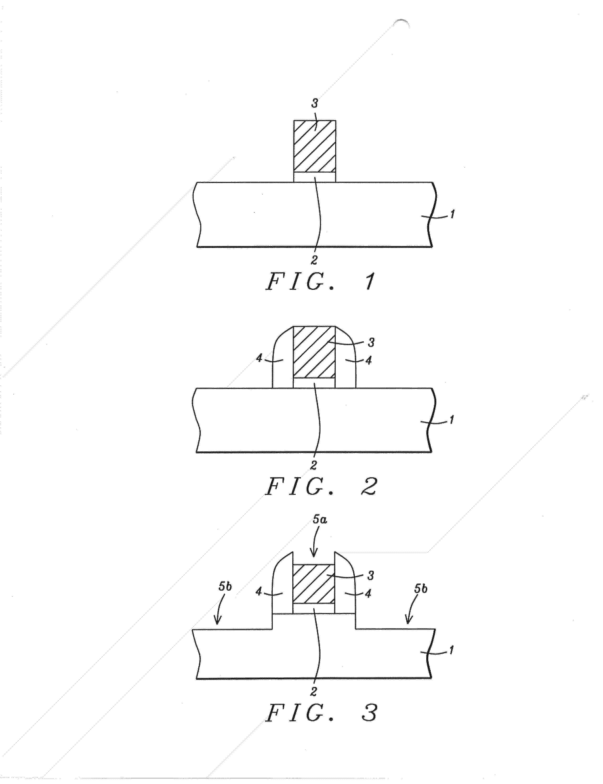
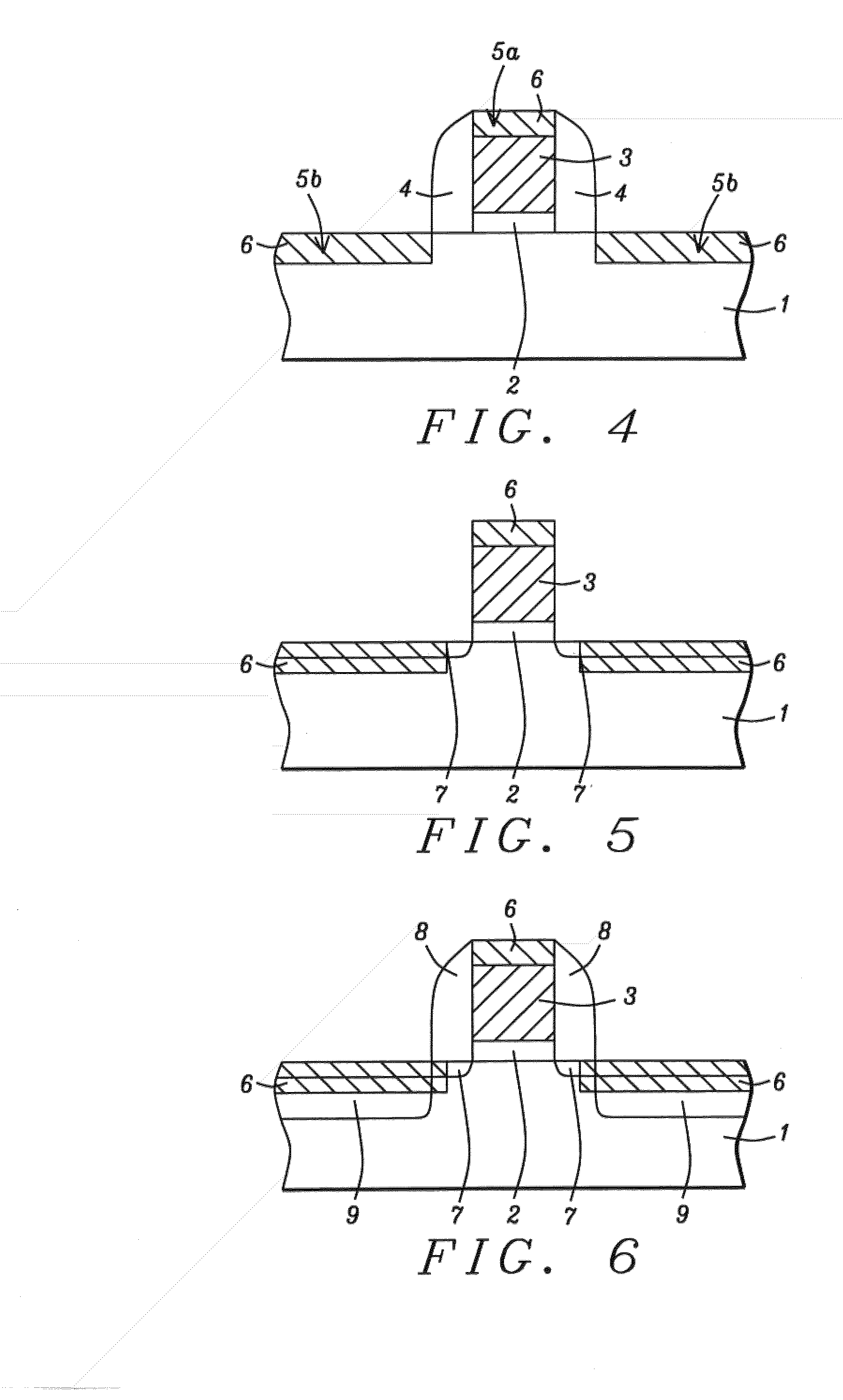
[0001] The present invention relates to methods used to fabricate semiconductor devices and more specifically to a method of fabricating a metal oxide semiconductor field effect (MOSFET) device featuring a channel region in a strained silicon region.
[0002] The ability to establish a channel region in a strained silicon region has allowed the performance of MOSFET devices to be enhanced. The increased mobility of carriers in the strained silicon region translates to increased drive currents thus enhanced device performance. Various options for creating the strained silicon region, or a silicon region under compressive strain, have been used such as forming the strained silicon layer directly on an underlying, relaxed silicon-germanium layer. Another option, practiced in the present invention, is the selective growth of relaxed silicon-germanium regions in an area of a semiconductor substrate to subsequently be used to accommodate a source / drain region. This...
PUM
 Abstract
Description
Claims
Application Information