Integration of photon emission microscope and focused ion beam

a technology of photon emission microscope and focused ion beam, which is applied in the direction of fault location by increasing the damage at fault, fluid pressure measurement, instruments, etc., can solve the problems of time-consuming and inefficient switching between a stand-alone pem and a fib machine, and many ic failures can be observed

Inactive Publication Date: 2006-01-19
DCG SYST
View PDF13 Cites 82 Cited by
  • Summary
  • Abstract
  • Description
  • Claims
  • Application Information

AI Technical Summary

Problems solved by technology

Many IC failures are can be observed as “hot spots”, i.e., spots where electroluminescence processes take place from failed devices exhibiting electrical current leakage.
The process outlined above is often iterative, i.e., requiring alternating between PEM and FIB tools multiple times. Switching between a stand-alone PEM and a FIB machine is time consuming and inefficient.

Method used


Image

  • Integration of photon emission microscope and focused ion beam
  • Integration of photon emission microscope and focused ion beam
  • Integration of photon emission microscope and focused ion beam

Examples


Embodiment Construction

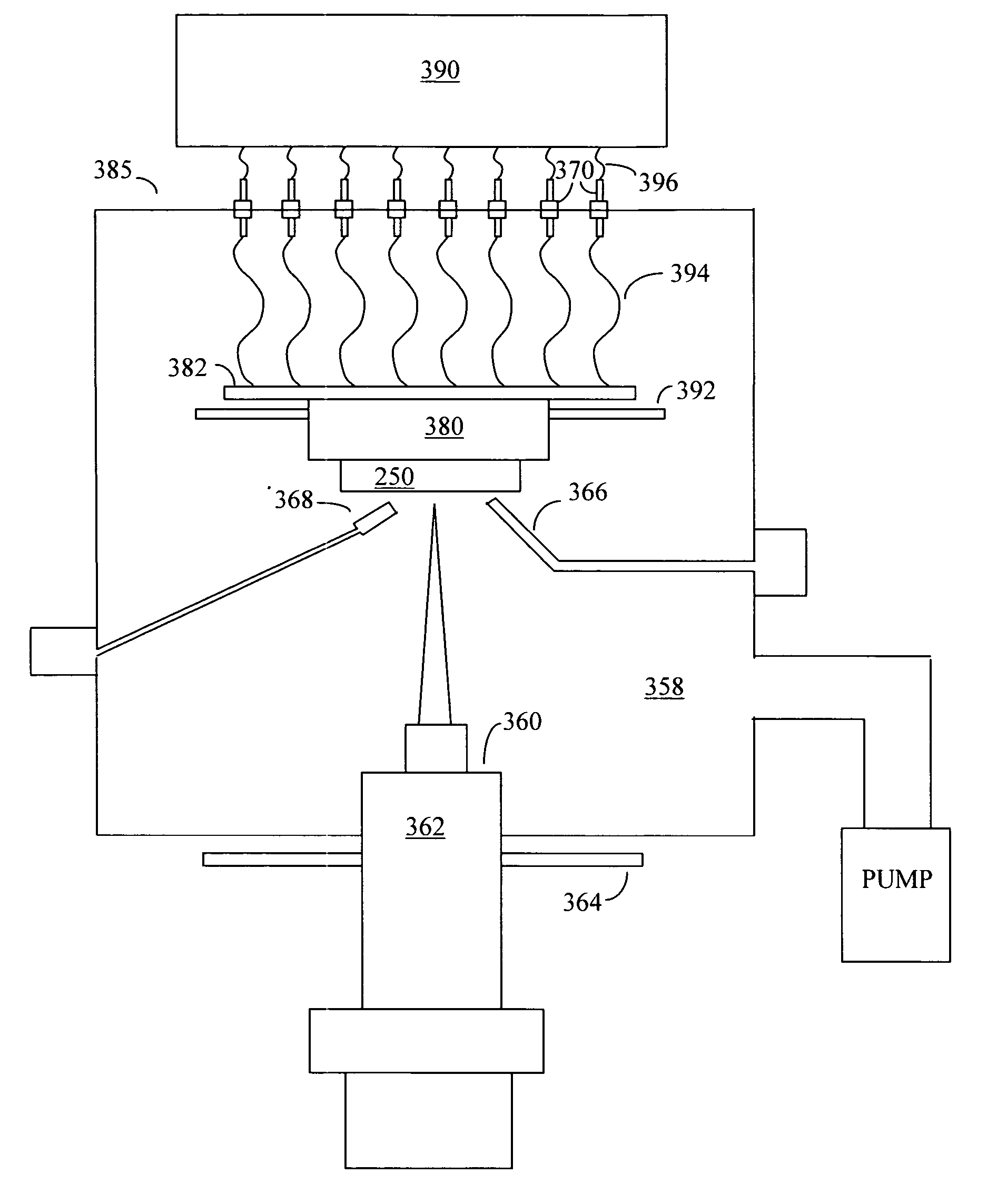
[0016] The present invention integrates a PEM with a FIB tool so as to accelerate FA. A FIB-optical dual beam system with a concentric beam axis is preferred, since the area of interest seen by both FIB and PEM is the same throughout the operation. The common focal plane of the FIB-optical dual beam system is also preferred, since it saves time in the FIB-PEM iteration process by minimizing the time of searching for features in the focal axis. For the convenience of direct comparison, field of view and magnification of both the optical and the FIB images should be adjusted so as to be identical, by adjusting the scan control voltages to the FIB electrostatic lenses. Simultaneous imaging is not required, but the capability of performing in-situ photon emission imaging as well as FIB circuit modification is required.

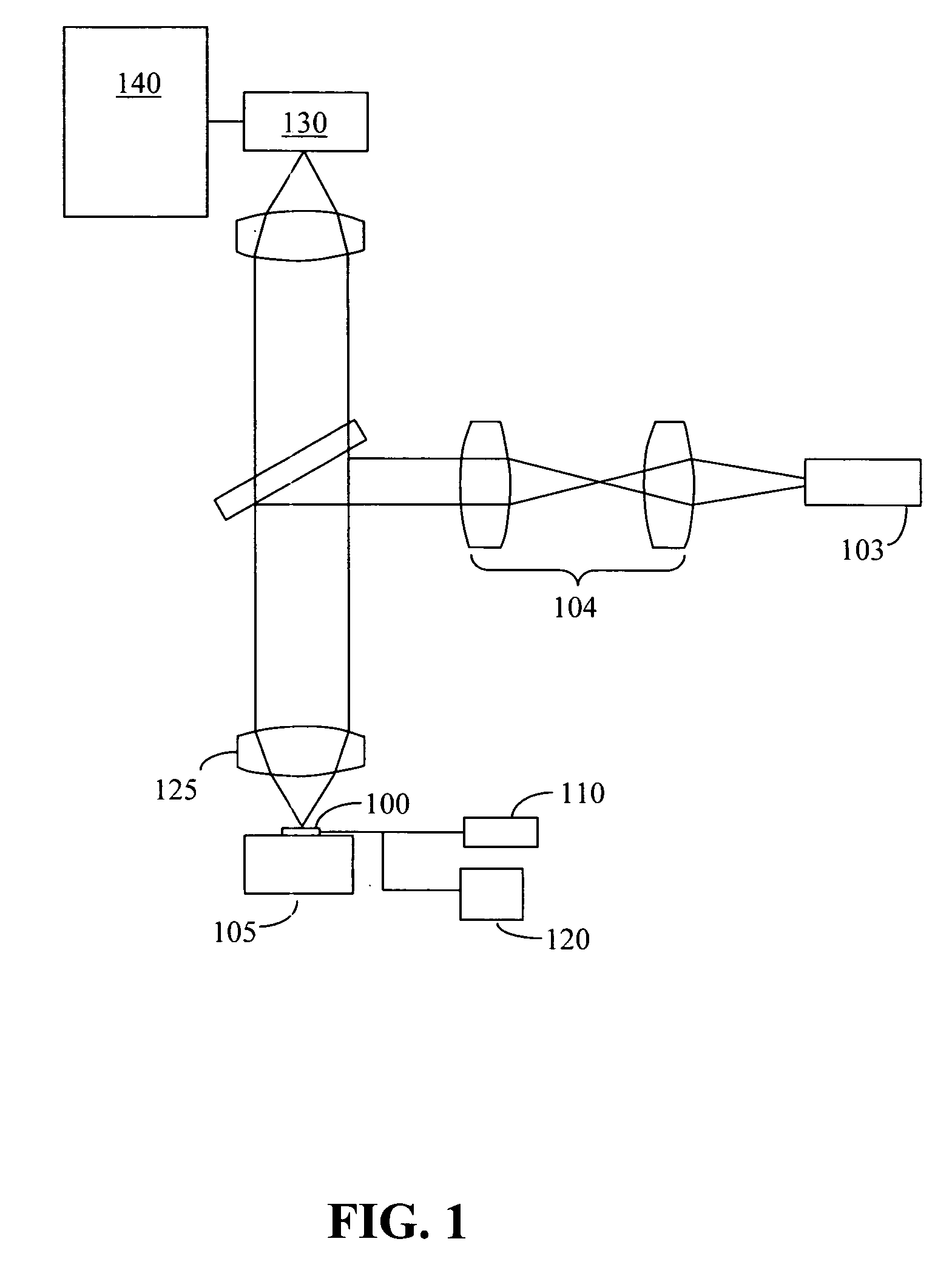
[0017] A Photon Emission Microscope, illustrated in FIG. 1, is a microscope designed for microscopic imaging of IC's with high detection efficiency with faint NIR emissio...


PUM


Abstract

An integrated FIB/PEM apparatus and method for performing failure analysis on integrated circuits. In-situ failure analysis is enabled by integrating Photon Emission Microscopy into a Focused Ion Beam system, thereby improving throughput and efficiency of Failure Analysis. An iterative method is described for identifying and localizing fault sites on the circuit.

Description

CROSS-REFERENCE TO RELATED APPLICATION [0001] This application claims priority from U.S. Provisional Application No. 60 / 587,327, filed Jul. 13, 2004.FIELD OF THE INVENTION [0002] This invention pertains to failure analysis for integrated circuits, and in particular to the integration of two important tools used in failure analysis, i.e., photon emission microscope, and focused ion beam. BACKGROUND OF THE INVENTION [0003] An important process component of integrated circuit manufacturing is Failure Analysis (FA). Generally FA is performed in response to customer returns, which are in turn in response to product failure issues which take place in the field. Additionally, FA is utilized for design debug, i.e., the analysis of failures due to imperfection of designing or processing, and feedback to circuit designers or processing fabs to correct the problem or to improve production yields. Many IC failures are can be observed as “hot spots”, i.e., spots where electroluminescence process...

Claims


Application Information

Patent Timeline
Patent Type & Authority Applications(United States)
IPC IPC(8): G01R31/302
CPCG01R31/302
Inventor TSAO, CHUN-CHENGDELENIA, EUGENE
Owner DCG SYST
Why Eureka
Try Eureka