

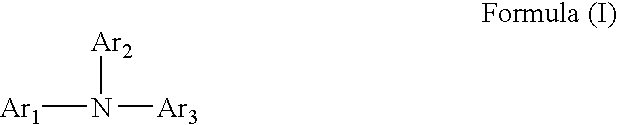
Organic electroluminescence device
a technology of electroluminescence device and organic material, which is applied in the direction of discharge tube luminescnet screen, other domestic articles, natural mineral layered products, etc., can solve the problems of increasing uneven luminance induced by voltage drop, loss of electroluminescent quantum yield with respect to current, and disadvantage of lowering emission luminance, so as to improve luminescent efficiency and durability. , the effect of reducing the driving voltag
- Summary
- Abstract
- Description
- Claims
- Application Information
AI Technical Summary
Benefits of technology
Problems solved by technology
Method used
Image


Examples
example 1
[0202]1. Preparation of Organic EL Device
[0203]A glass substrate having a thickness of 0.7 mm was subjected to ultrasonic cleaning in 2-propanol and treated with UV and ozone for 20 minutes. Then, aluminum was deposited thereon as an anode by vacuum deposition to a thickness of 60 nm, and organic layers were deposited sequentially thereon by vapor deposition, to prepare a laminate having two emission units in the following configuration.
[0204]
[0205]“glass substrate / anode: Al (60 nm) / light emission unit A / n-doped layer / alkali metal layer / layer containing hole transport material / p-doped layer / light emission unit B / cathode: Ag (15 nm)”
[0206]The light emission unit A: a laminate formed by a N,N′-dinaphthyl-N,N′-diphenyl-[1,1′-biphenyl]-4,4′-diamine (which is referred to hereinafter as “α-NPD” in some cases) layer deposited at the thickness of 10 nm as a hole transport layer / a co-deposited layer of 4,4′-di-(N-carbazole)-biphenyl (which is referred to hereinafter as “CBP” in some cases) a...
PUM
| Property | Measurement | Unit |
|---|---|---|
| glass transition point | aaaaa | aaaaa |
| ionization potential | aaaaa | aaaaa |
| thickness | aaaaa | aaaaa |
Abstract
Description
Claims
Application Information