Organic electroluminescence element

a technology of electroluminescence elements and organic materials, applied in the direction of discharge tubes/lamp details, discharge tubes luminescnet screens, organic semiconductor devices, etc., can solve the problems of increasing driving voltage, lowering brightness, and many problems for putting organic electroluminescence elements to practical use, so as to improve external quantum efficiency, improve durability, and reduce driving voltage

Active Publication Date: 2008-07-24
UDC IRELAND
View PDF6 Cites 3 Cited by
  • Summary
  • Abstract
  • Description
  • Claims
  • Application Information

AI Technical Summary

Benefits of technology

[0128]In a case where the hole injection layer contains an acceptor, it is preferred that the hole transport layer has no substantial acceptor.
[0129]Although a thickness of the hole injection layer and the hole transport layer is not particularly limited, it is preferred that the thickness is 1 nm to 5 μm, it is more preferably 5 nm to 1μm, and 10 nm to 500 nm is particularly preferred in view of decrease in driving voltage, improvements in external quantum efficiency, and improvements in durability.
[0130]The hole injection layer and the hole transport layer may be composed of a mono-layered structure comprising one or two or more of the above-mentioned materials, or a multilayer structure composed of plural layers of a homogeneous composition or a heterogeneous composition.
[0131]When the carrier transportation layer adjacent to the light emitting layer is a hole transport layer, it is preferred that the Ip (HTL) of the hole transport layer is smaller than the Ip (D) of the dopant contained in the light emitting layer in view of driving durability.
[0132]The Ip value in the present invention is determined by measuring with a UV PHOTO-ELECTRON ANALYZER AC-1 (manufactured by Riken Keiki Co., Ltd.) under room temperature in atmosphere. A fundamental principle of a measurement by the AC-1 is described, for example, in “DATA BOOK OF WORK FUNCTION ABOUT ORGANIC THIN FILMS” authored by CHIHAYA ADACHI et al., published by CMC Publishing Co., Ltd, in 2004.
[0133](Electron Injection Layer and Electron Transport Layer)

Problems solved by technology

However, many problems still remain for putting organic electroluminescence elements to practical use.
However, this means potentially involves a problem of lowering the brightness and increasing the driving voltage since the migration of all of the carriers is lowered, as well as a problem of lowering the driving durability, since the time that the carriers stay in the device is made longer.
However, in this configuration, since the insulation layer and the electrode between the light emitting units hinder the extraction of light emission, light emitted from each of the light emitting units cannot substantially be utilized sufficiently.
Further, this is not a means for improving the low external quantum efficiency inherent to each of the light emitting units.
However, in this configuration as well, the light emitting units are merely stacked in a plurality, and this cannot provide a means for improving the low external quantum efficiency inherent to each of the light emitting units.

Method used


Image

  • Organic electroluminescence element
  • Organic electroluminescence element
  • Organic electroluminescence element

Examples


example 1

1. Preparation of Organic EL Element

[0196](Preparation of Comparative Organic EL Element No. A)

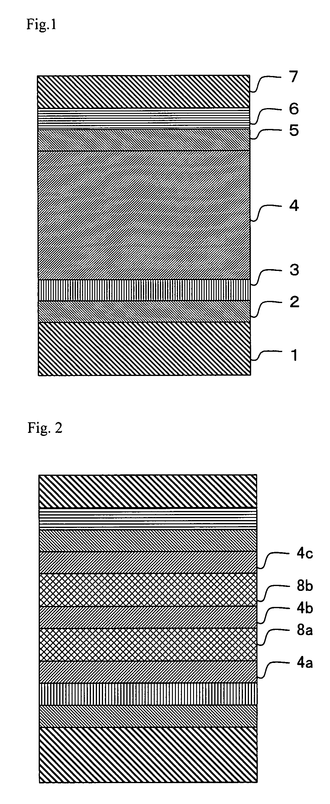
[0197]A 2.5 cm square ITO glass substrate having a 0.5 mm thickness (manufactured by Geomatec Co., Ltd.; surface resistance: 10 Ω / □) was placed in a washing container to apply ultrasonic cleaning in 2-propanol, and then, UV-ozone treatment was applied for 30 minutes. On this transparent anode, the following layers were deposited in accordance with a vacuum deposition method. In the examples of the present invention, a deposition rate was 0.2 nm / second, unless otherwise specified, wherein the deposition rate was measured by the use of a quartz oscillator. The thicknesses of layers described below were also measured by using the quartz oscillator.

[0198]—Hole Injection Layer—

[0199]On the ITO layer, CuPc was deposited by the evaporation method at a thickness of 10 nm.

[0200]—Hole Transport Layer—

[0201]On the hole injection layer, α-NPD was deposited by the evaporation method at a thickness of 3...

example 2

1. Preparation of Organic EL Element

[0220](Preparation of Comparative Organic EL Element No. C)

[0221]A comparative organic EL element No. C was manufactured in the same manner as the comparative organic EL element No. A except for changing the light emitting layer to the following composition.

[0222]Light emitting layer: mCP and Ir(ppy)3 were co-deposited at a volume ratio of 95:5. The thickness of the light emitting layer was 140 nm.

(Preparation of Comparative Organic EL Element No. D)

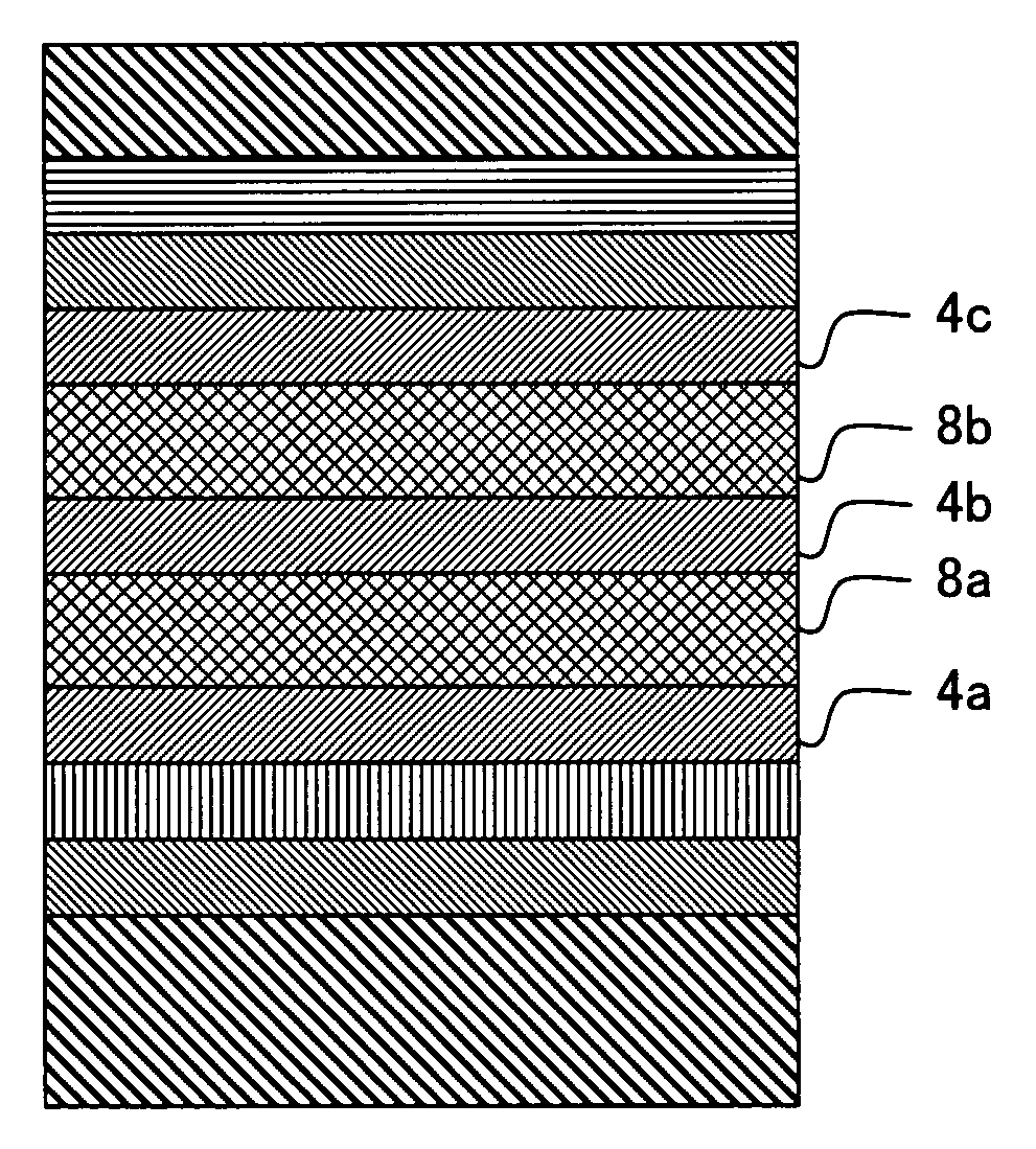
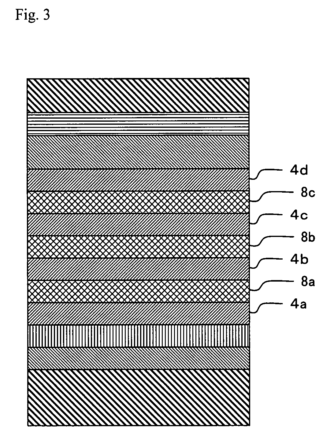
[0223]In the process of preparing the comparative organic EL device No. C, the light emitting layer was divided into the following four unit light emitting layers, and the following intermediate layers 11 to 13 were disposed between the respective unit light emitting layers. In order from the hole transport layer, the respective unit light emitting layer 11 / intermediate layer 13 / unit light emitting layer 12 / intermediate layer 12 / unit light emitting layer 13 / intermediate layer 11 / unit light emitting lay...


PUM


Abstract

An organic electroluminescence element includes at least a light-emitting layer between a pair of electrodes, wherein the light-emitting layer is divided into at least three layers, an intermediate layer containing an electron blocking material or a hole blocking material is disposed between the divided light-emitting layers, an Ea value of the electron blocking material is smaller than an Ea value of a host material of the divided light-emitting layer adjacent on a cathode side or an Ip value of the hole blocking material is larger than an Ip value of a host material of the divided light-emitting layer adjacent on the anode side of the intermediate layer, and a difference of ΔEa or ΔIp is controlled to specific range.

Description

CROSS-REFERENCE TO RELATED APPLICATION[0001]This application claims priority under 35 USC 119 from Japanese Patent Application No. 2006-265987, the disclosure of which is incorporated by reference herein.BACKGROUND OF THE INVENTION[0002]1. Field of the Invention[0003]The present invention relates to an organic electroluminescence element which has improved external quantum efficiency, and in particular, to an organic electroluminescence element which can be effectively applied to a surface light source for a full color display, a backlight, an illumination light source or the like; or a light source array for a printer or the like.[0004]2. Description of the Related Art[0005]An organic electroluminescence element (hereinafter, referred to as an “organic EL element” in some cases) is composed of a light emitting layer or a plurality of functional layers containing a light emitting layer, and a pair of electrodes sandwiching these layers. The organic electroluminescence element is a d...

Claims


Application Information

Patent Timeline
Patent Type & Authority Applications(United States)
IPC IPC(8): H01J1/63
CPCC09K11/06H05B33/14C09K2211/1011C09K2211/1014C09K2211/1029C09K2211/1033C09K2211/1044C09K2211/1088C09K2211/1092C09K2211/182C09K2211/185H01L51/006H01L51/0067H01L51/0071H01L51/0085H01L51/0089H01L51/5012H01L51/5016H01L51/5096H01L51/5237H01L51/5265H01L51/5278H01L2251/552C09K2211/1007H10K85/633H10K85/351H10K85/654H10K85/657H10K85/342H10K50/18H10K50/11H10K2101/10H10K50/852H10K50/19H10K50/844H10K2101/30H10K50/84
Inventor KINOSHITA, MASARUTOBISE, MANABU
Owner UDC IRELAND
Why Eureka
Try Eureka