Organic electroluminescence device

Inactive Publication Date: 2007-06-14
UDC IRELAND
View PDF8 Cites 9 Cited by
  • Summary
  • Abstract
  • Description
  • Claims
  • Application Information

AI Technical Summary

Benefits of technology

[0048] Although an applied amount of these electron-accepting dopants depends on the type of material, 0.01% by mass to 50% by mass of a dopant is preferred with respect to a positive hole-transport layer material, 0.05% by mass to 20% by mass is more preferable, and 0.1% by mass to 10% by mass is particularly preferred. When the amount applied is less than 0.01% by mass with respect to the positive hole transportation material, it is not desirable because the advantageous effects of the present invention are insufficient, and when it exceeds 50% by mass, positive hole transportation ability is deteriorated, and thus, this is not preferred.
[0049] As a material for the positive hole-injection layer and the positive hole-transport layer, it is preferred to contain specifically pyrrole derivatives, carbazole derivatives, pyrazole derivatives, triazole derivatives, oxazole derivatives, oxadiazole derivatives, imidazole derivatives, polyarylalkane derivatives, pyrazoline derivatives, pyrazolone derivatives, phenylenediamine derivatives, arylamine derivatives, amino-substituted calcon derivatives, styrylanthracene derivatives, fluorenone derivatives, hydrazone derivatives, stilbene derivatives, silazane derivatives, aromatic tertiary amine compounds, styrylamine derivatives, aromatic dimethylidine compounds, porphyrin compounds, organosilane derivatives, carbon or the like.
[0050] Although a thickness of the positive hole-injection layer and the positive hole-transport layer is not particularly limited, it is preferred that the thickness is 1 nm to 5 μm, it is more preferably 5 nm to 1 μm, and 10 nm to 500 nm is particularly preferred in view of decrease in driving voltage, improvements in luminescent efficiency, and improvements in durability.
[0051] The positive hole-injection layer and the positive hole-transport layer may be composed of a monolayered structure comprising one or two or more of the above-mentioned materials, or a multilayer structure composed of plural layers of a homogeneous composition or heterogeneous compositions.
[0052] When the carrier transportation layer adjacent to the light-emitting layer is a positive hole-transport layer, it is preferred that the Ip (HTL) of the positive hole-transport layer is smaller than the Ip (D) of the dopant contained in the light-emitting layer in view of driving durability.
[0053] The Ip (HTL) in the positive hole-transport layer may be measured in accordance with the below-mentioned measuring method of Ip.

Problems solved by technology

However, there are still many technical problems to overcome, such as with respect to luminescence brightness and color tone, durability under various ambient operating conditions, and mass productivity at low cost, in order for these devices to be practically used in these fields in place of conventional display devices.
However, the method has only resulted in increase in light loss due to absorption and scattering during the process of the lights emitted in respective light-emitting layers transmitting through other light-emitting layers, and thus, an effect of combining the lights by lamination has not been sufficiently obtained.
However, the device only has a single light-emitting layer, which imposes limitations on high-brightness light emission.

Method used


Image

  • Organic electroluminescence device
  • Organic electroluminescence device
  • Organic electroluminescence device

Examples


example 1

[0179] A glass substrate having a thickness of 0.7 mm was subjected to ultrasonic cleaning in 2-propanol and treated with UV and ozone for 20 minutes. Then, silver was deposited thereon as an anode by vacuum deposition to a thickness of 15 nm, and organic layers were deposited sequentially thereon by vapor deposition, to prepare a laminated film having two emission units in the following configuration.

[0180]

[0181] Glass substrate / Ag (15 nm) / 2-TNATA+33-% by mass of V2O5 (20 nm) / 2-TNATA+0.1-% by mass of F4-TCNQ (110 nm) / α-NPD (10 nm) / CBP+5-% by mass of tbppy (20 nm) / BAlq (10 nm) / Alq (20 nm) / LiF (0.5 nm) / Al(1.5 nm) / 2-TNATA+33-% by mass of V2O5 (20 nm) / 2-TNATA+0.1-% by mass of F4-TCNQ (43nm) / α-NPD (10 nm) / CBP+5-% by mass of tbppy (20 nm) / BAlq (10 nm) / Alq(32 nm) / LiF (0.5 nm) / Al (100 nm)

[0182] In the expression above, the term “+” in 2-TNATA+V2O5, 2-TNATA+F4-TCNQ, and CBP+tbppy (light-emitting layer) means that the compounds were co-deposited.

[0183] An emission area of 50 mm×50 mm in...

example 2

[0194] A device was prepared in a similar manner to Example 1, except that the distance between light-emitting layers was changed from 125 nm to 170 nm while the total thickness of the layers was preserved.

[0195]

[0196] Glass substrate / Ag (15 nm) / 2-TNATA+33-% by mass of V2O5 (20 nm) / 2-TNATA+0.1-% by mass of F4-TCNQ (65 nm) / α-NPD (10 nm) / CBP+5-% by mass of tbppy(20 nm) / BAlq (10 nm) / Alq (20 nm) / LiF (0.5 nm) / Al (1.5 nm) / 2-TNATA+33-% by mass of V2O5 (20 nm) / 2-TNATA+0.1-% by mass of F4-TCNQ (88 nm) / α-NPD (10 nm) / CBP+5-% by mass of tbppy (20 nm) / BAlq (10 nm) / Alq (32 nm) / LiF (0.5 nm) / Al (100 nm)

[0197] The device obtained was evaluated in a similar manner to Example 1. The results are shown in Table 1. The peak intensity declined slightly, compared to that in Example 1, but light emission that was sharper in emission spectrum than that in the Comparative Examples was obtained.

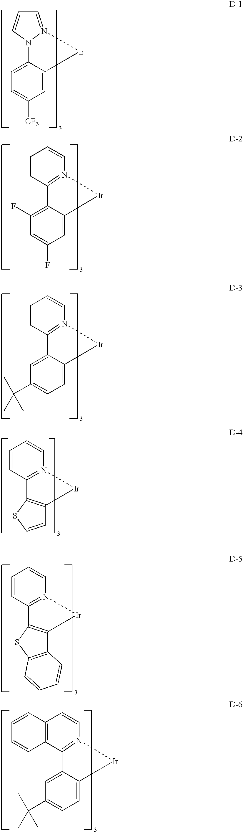
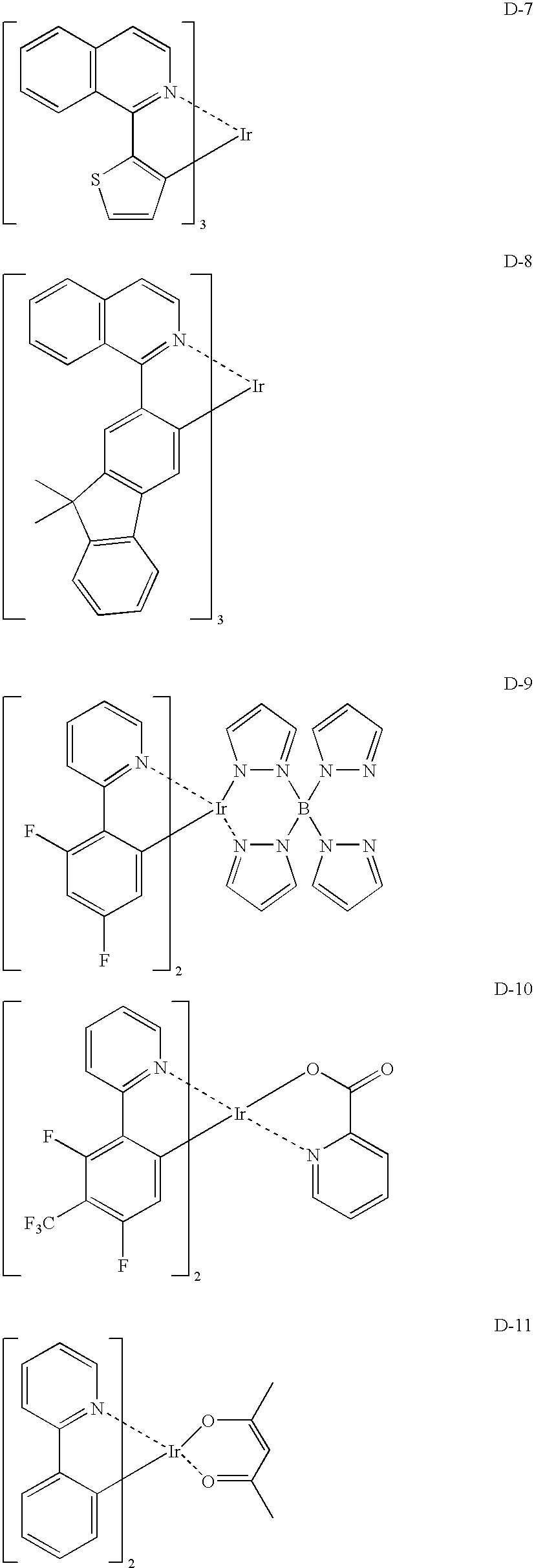
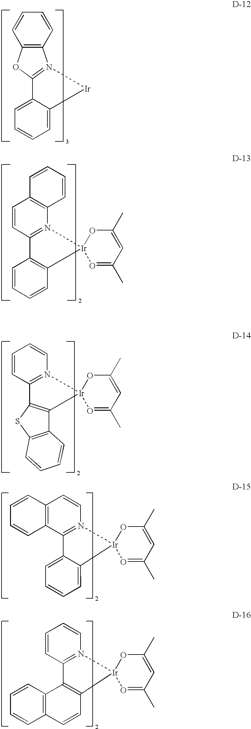
[0198] Structures of the compounds used in the above-described luminescent devices are shown below.

TABLE 1Pea...


PUM


Abstract

An organic electroluminescence device, comprising multiple light-emitting layers laminated between a pair of electrodes, wherein an electrode on a side where emitted light is outgoing from the light-emitting layer is a translucent and half-reflective metal electrode. According to the present invention, an organic electroluminescence device having a multi-photon device structure that is improved in light withdrawal efficiency and obtains high-brightness light emission is provided. Furthermore, an organic electroluminescence device which exhibits high-brightness light emission, and which is superior in directivity and low in brightness irregularity.

Description

CROSS-REFERENCE TO RELATED APPLICATION [0001] This application claims priority under 35 USC 119 from Japanese Patent Application No. 2005-354668, the disclosure of which is incorporated by reference herein. BACKGROUND OF THE INVENTION [0002] 1. Field of the invention [0003] The invention relates to an organic electroluminescence device which obtains high-brightness light emission, and in particular, to an organic electroluminescence device that is superior in directivity and low in brightness irregularity. [0004] 2. Description of the Related Art [0005] Organic electroluminescence devices containing a thin film material that emits light by excitation due to application of electric current have been known. The organic electroluminescence devices, which obtain high-brightness light emission at low voltage, have broad potential applications in fields such as cellular phone displays, personal digital assistants (PDA), computer displays, car information displays, TV monitors, and general...

Claims


Application Information

Patent Timeline
IPC IPC(8): H01J1/62H01J63/04
CPCH01L51/0085H01L51/5052H01L51/5265H01L51/5278H10K85/342H10K50/155H10K50/165H10K50/852H10K50/19
Inventor KINOSHITA, MASARUNAKAYAMA, MASAYA
Owner UDC IRELAND
Why Eureka
Try Eureka