
Field emission display

Inactive Publication Date: 2006-04-25
SAMSUNG SDI CO LTD
View PDF15 Cites 10 Cited by
  • Summary
  • Abstract
  • Description
  • Claims
  • Application Information

AI Technical Summary

Benefits of technology

[0021]In accordance with an embodiment of the present invention a field emission display is provided in which electric field emission areas around emitters are increased and a strength of electric fields applied to emitters is increased such that a drive voltage of the display may be decreased and electron emission amounts of the emitters may be increased.
[0023]In accordance with still another embodiment of the present invention a field emission display is provided in which electron beam dispersion is minimized such that electron beams emitted from emitters selectively illuminate phosphor layers of only intended pixels, thereby improving picture quality.
[0024]In accordance with yet another embodiment of the present invention a field emission display is provided in which a high voltage is applied to an anode electrode while reducing the possibility of arcing between cathode electrodes and an anode electrode, thereby improving screen brightness.

Problems solved by technology

As a result, compared to the FED using the conventional triode structure, the electric field intensity around emitters 9 is significantly lower, and the drive voltage and power consumption required for electron emission is high since the area of field emission is limited.
Also, because of this small area of field emission, the amount of electrons that are emitted is small such that there are limitations in increasing screen brightness.
In addition, although brightness is maintained in the case where a white color is displayed on the screen, if colors are displayed, these areas may become dark such that uneven brightness occurs in the picture.
However, if cathode electrodes 7 are positioned too closely, the data voltage applied to cathode electrodes 7 is cut off by adjacent cathode electrodes 7 such that an increase in the electric field of corresponding emitters 9 is unable to be realized.
Therefore, the control of field emission by gate electrodes 3 is not possible, thereby making matrix driving unattainable.
Color purity is reduced as a result and precise images are unable to be realized.
This results in damage or heating of emitters 9 such that uniformity in the illumination of the screen is reduced and the lifespan of the emitters deteriorates.

Method used


Image

  • Field emission display
  • Field emission display
  • Field emission display

Examples


first embodiment

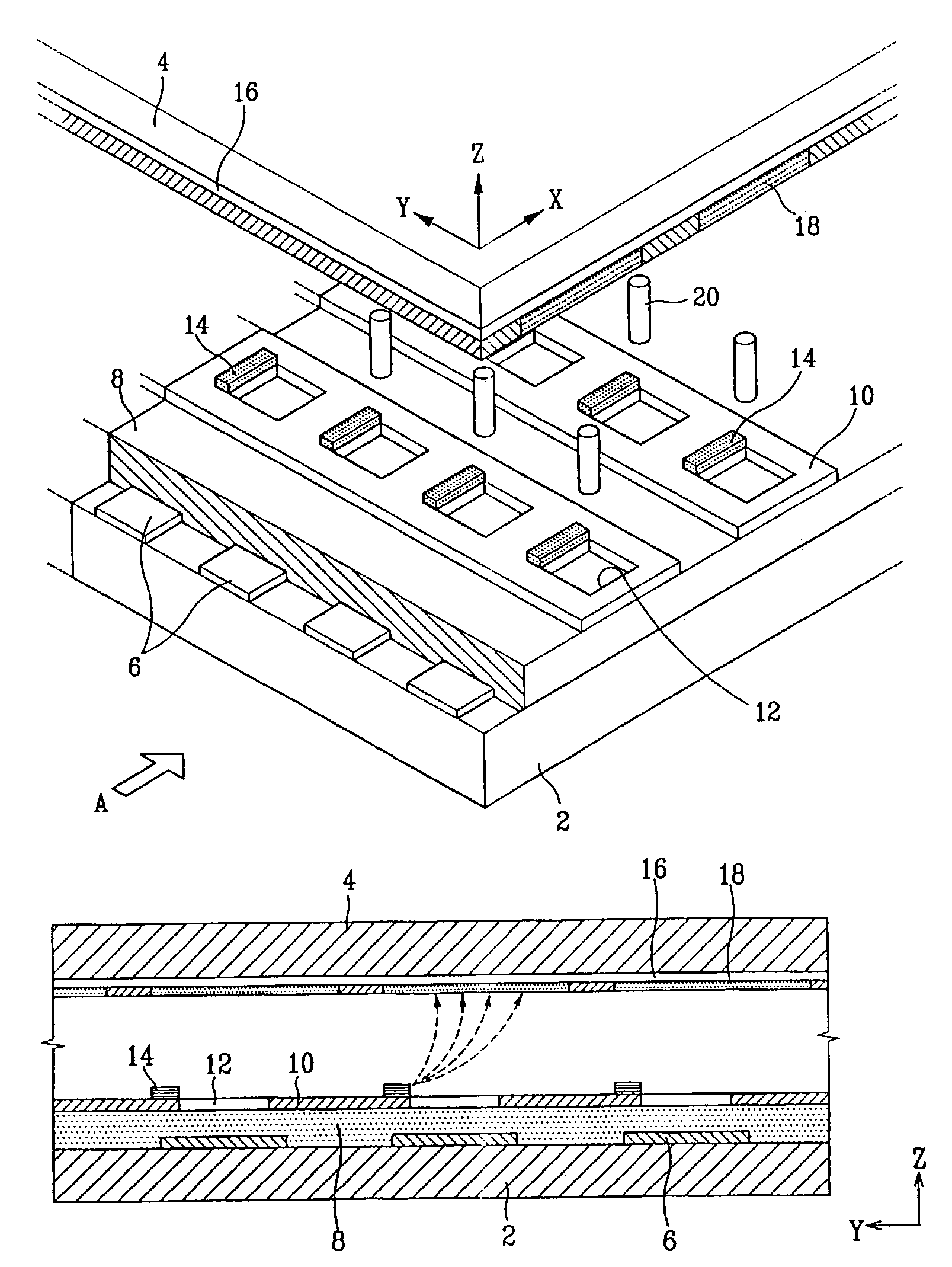
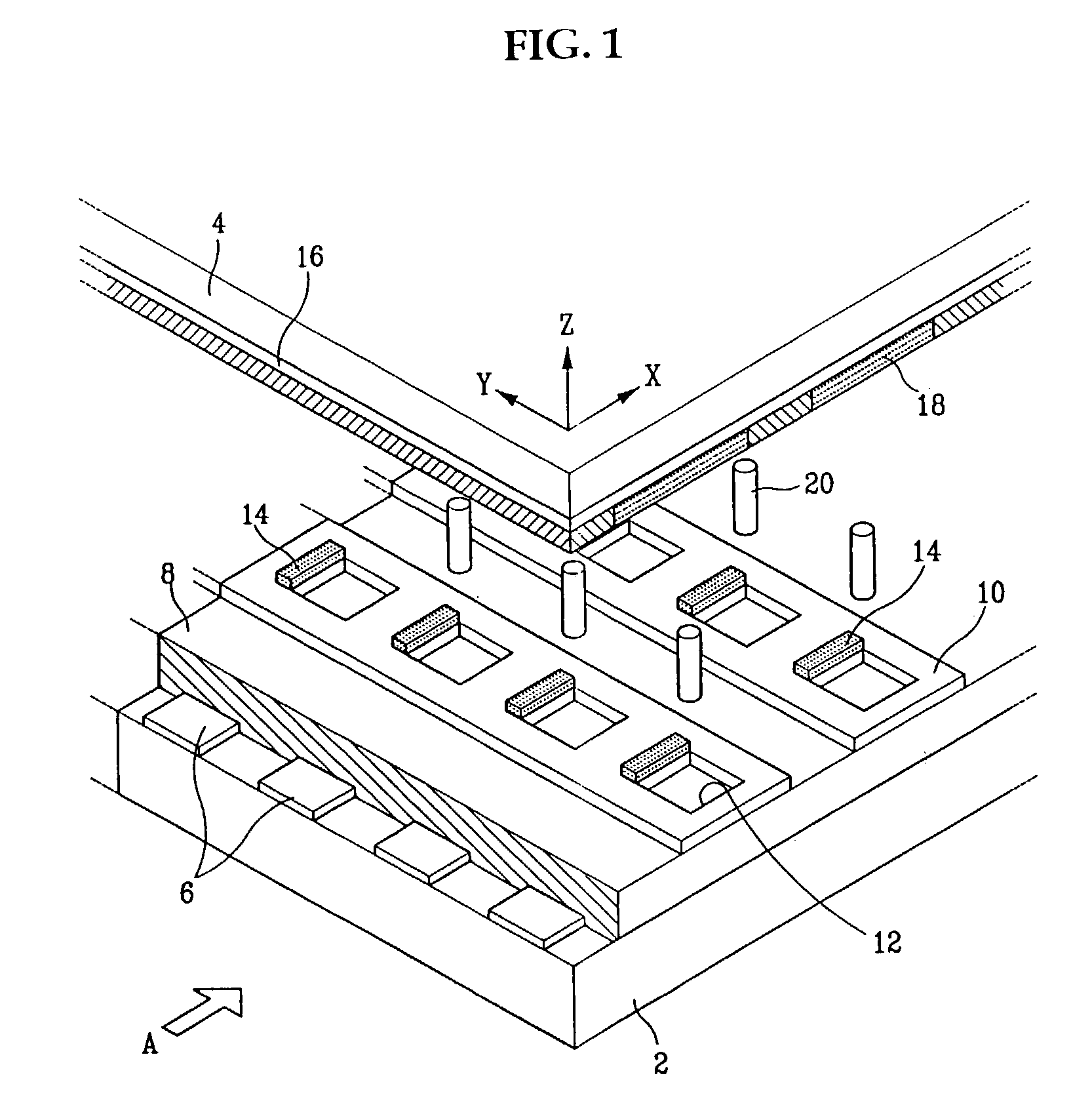
[0061]FIG. 1 is a partial exploded perspective view of a field emission display according to the present invention, and FIG. 2 is a partial sectional view of the field emission display of FIG. 1 as viewed from direction A and shown in an assembled state.

[0062]As shown in the drawings, the field emission display (FED) includes first substrate 2 of predetermined dimensions (hereinafter referred to as a rear substrate) and second substrate 4 of predetermined dimensions (hereinafter referred to as a front substrate). Front substrate 4 is provided opposing rear substrate 2 with a predetermined gap therebetween. A structure to enable the emission of electrons by forming an electric field is provided on rear substrate 2 and a structure to enable the realization of predetermined images by the interaction with emitted electrons is provided on front substrate 4.

[0063]In more detail, at least one gate electrode 6, especially a plurality of gate electrodes 6 are formed on rear substrate 2 in a ...

second embodiment

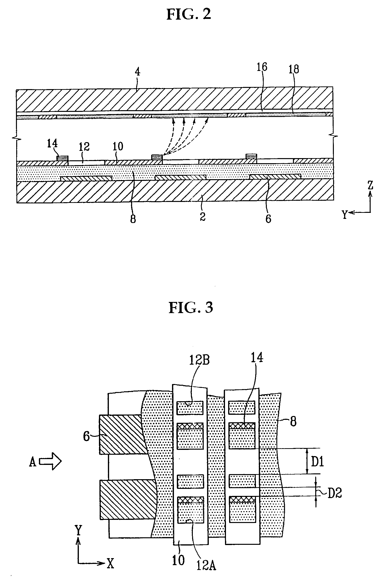
[0073]FIG. 3 is a partial plan view of a rear substrate of a field emission display according to the present invention, and FIG. 4 is a partial sectional view of the field emission display of FIG. 3 as viewed from direction A and shown in an assembled state.

[0074]As shown in the drawings, main field enhancing section 12A and auxiliary field enhancing section 12B are formed in pairs in cathode electrodes 10 at areas corresponding to each pixel region and along cathode electrodes 10 (in an axis Y direction of the drawings). Emitters 14 are positioned on cathode electrodes 10 adjacent to one edge of main field enhancing sections 12A. That is, for each pair of main field enhancing sections 12A and auxiliary field enhancing sections 12B, an emitter 14 is positioned adjacent to one of the edges of the main field enhancing section 12A that is closest its paired auxiliary field enhancing section 12B.

[0075]Main field enhancing sections 12A and auxiliary field enhancing sections 12B are forme...

third embodiment

[0077]FIG. 5 is a partial plan view of a rear substrate of a field emission display according to the present invention, and FIG. 6 is a partial sectional view of the field emission display of FIG. 5 as viewed from direction A and shown in an assembled state.

[0078]Using the basic structure of the second embodiment, the FED further includes counter electrodes 22 formed in main field enhancing sections 12. Counter electrodes 22 are connected to gate electrodes 6. That is, via hole 8a is formed in each of the main field enhancing sections 12A passing through insulation layer 8, and one of the counter electrodes 22 is formed in each of the main field enhancing sections 12A covering and passing through the corresponding via hole 8a to contact the corresponding gate electrode 6.

[0079]When a predetermined drive voltage is applied to gate electrodes 6 to form electric fields between gate electrodes 6 and emitters 14 for electron emission, counter electrodes 22 act to attract the voltage of g...


PUM


Abstract

A field emission display includes a first substrate and a second substrate opposing one another with a predetermined gap therebetween. At least one gate electrode is formed on the first substrate. An insulation layer formed over the first substrate covering the gate electrode. Cathode electrodes are formed on the insulation layer and including field enhancing sections that expose the insulation layer corresponding to pixel regions. Electron emission sources formed over the cathode electrodes adjacent at least one side of the field enhancing sections. An illumination assembly is formed on the second substrate and realizes the display of images by electrons emitted from the electron emission sources.

Description

CROSS-REFERENCE TO RELATED APPLICATIONS[0001]This application claims priority to and the benefit of Korean Application Nos. 2002-20004, 2002-21964, 2002-78780, and 2002-79225, respectively filed on Apr. 12, 2002, Apr. 22, 2002, Dec. 11, 2002, and Dec. 12, 2002 in the Korean Industrial Property Office, the entire disclosures of which are incorporated herein by reference.BACKGROUND OF THE INVENTION[0002](a) Field of the Invention[0003]The present invention relates to field emission displays (FEDs). More particularly, the present invention relates to FEDs that include electron emission sources made of carbon-based material.[0004](b) Description of the Related Art[0005]In modern FEDs, a thick-layer process such as screen printing is used to form electron emission sources (i.e., emitters) in a flat configuration utilizing a carbon-based material that emits electrons at low voltage driving conditions (e.g., 10–100V).[0006]Carbon-based materials suitable for forming the emitters include gr...

Claims


Application Information

Patent Timeline
IPC IPC(8): H01J19/24H01J1/304H01J31/12
CPCH01J31/127
Inventor LEE, CHUN-GYOOLEE, SANG-JOCHOI, YONG-SOOAHN, SANG-HYUCKLEE, BYONG-GONHAN, HO-SU
Owner SAMSUNG SDI CO LTD
Learn More