Organic electroluminescence element
a technology of electroluminescence element and organic light, which is applied in the direction of discharge tube/lamp details, discharge tube luminescnet screen, organic semiconductor device, etc., can solve the problems of increasing driving voltage, lowering brightness, and many problems for putting organic el elements to practical use, so as to improve luminescent efficiency and durability. , the effect of reducing the driving voltag
- Summary
- Abstract
- Description
- Claims
- Application Information
AI Technical Summary
Benefits of technology
Problems solved by technology
Method used
Image
Examples
example 1
1. Preparation of Organic EL Element
(Preparation of Comparative Organic EL Element No. 1)
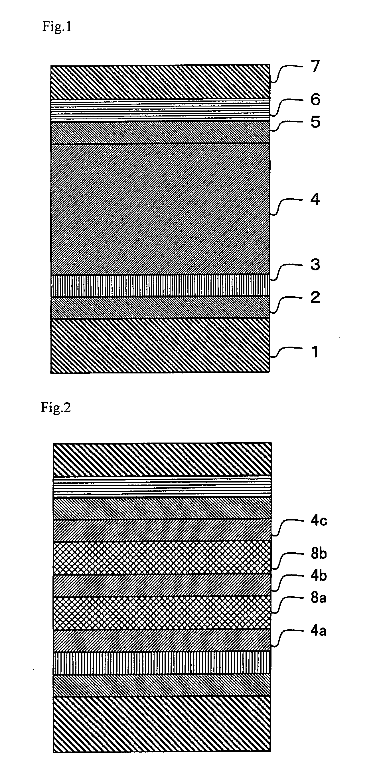
[0195]A 2.5 cm square ITO glass substrate having a 0.5 mm thickness (manufactured by Geomatec Co., Ltd.; surface resistance: 10 Ω / □) was placed in a washing container to apply ultrasonic cleaning in 2-propanol, and then, UV-ozone treatment was applied for 30 minutes. On this transparent anode, the following layers were deposited in accordance with a vacuum deposition method. In the examples of the present invention, a deposition rate was 0.2 nm / second, unless otherwise specified, wherein the deposition rate was measured by the use of a quartz oscillator. The thicknesses of layers described below were also measured by using the quartz oscillator.
[0196]—Hole Injection Layer—
[0197]On the ITO layer, CuPc was deposited by the evaporation method at a thickness of 10 nm.
[0198]—Hole Transport Layer—
[0199]On the hole injection layer, α-NPD was deposited by the evaporation method at a thickness of 10 nm.
[...
example 2
1. Preparation of Organic EL Element No. 2 of the Invention
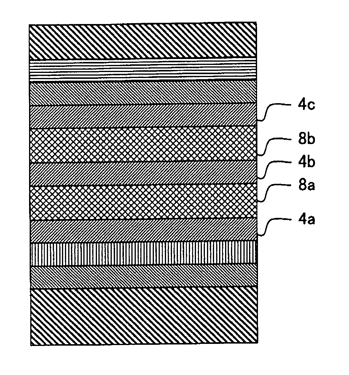
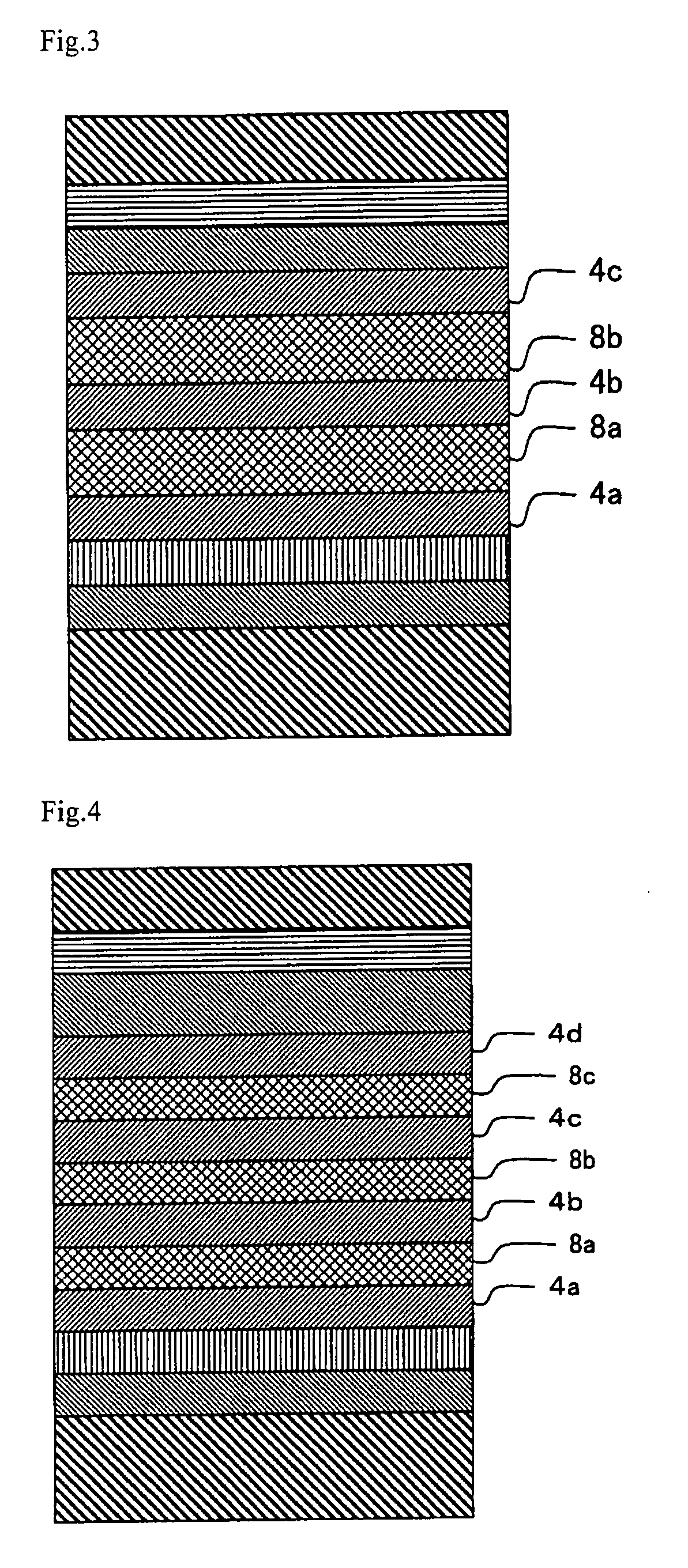
[0230]In the process preparing the comparative organic electroluminescence element No. 1, the light emitting layer was divided into 4 unit light emitting layers as shown below, and between the respective unit light emitting layers, intermediate layers 11 to 13 described below were disposed. Sequentially, from a hole transport layer, a unit light emitting layer 11 / an intermediate layer 11 / a unit light emitting layer 12 / an intermediate layer 12 / a unit light emitting layer 13 / an intermediate layer 13 / a unit light emitting layer 14 were disposed.
[0231]Unit light emitting layers 11 to 14: a composition the same as that of the light emitting layer of comparative organic EL element No. 1 was vapor deposited at the thickness of 15 nm for each layer.
[0232]Intermediate Layers 11, 12 and 13:
[0233]An electron transporting material B and Ir(ppy)3 were co-deposited at a volume ratio of 95:5 to form an intermediate layer.
[0234]The thickne...
example 3
1. Preparation of Organic EL Element No. 3
[0240]In the process of preparing Example 2, intermediate layers having an electron blocking capacity, each having the following composition, were used as the intermediate layers.
[0241]Sequentially, from a hole transport layer, unit light emitting layer 21, intermediate layer 21, unit light emitting layer 22, intermediate layer 22, unit light emitting layer 23, intermediate layer 23 and unit light emitting layer 24 were disposed.
[0242]Each of the unit light emitting layers 21 to 24 had the same composition as the light emitting layer in the comparative organic EL element No. 1, and was vapor-deposited to have a thickness of 15 nm.
[0243]The intermediate layers 21 to 23 respectively contained hole transport materials A to C together with Ir(ppy)3, where the hole transport material / Ir(ppy)3 volumetric ratio was set at 95:5.
[0244]Intermediate layer 21:
[0245]Intermediate layer 22:
[0246]Intermediate layer 23:
[0247]Each of the intermediate layer...
PUM
 Abstract
Description
Claims
Application Information


