

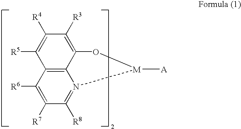
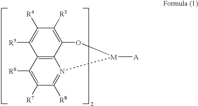
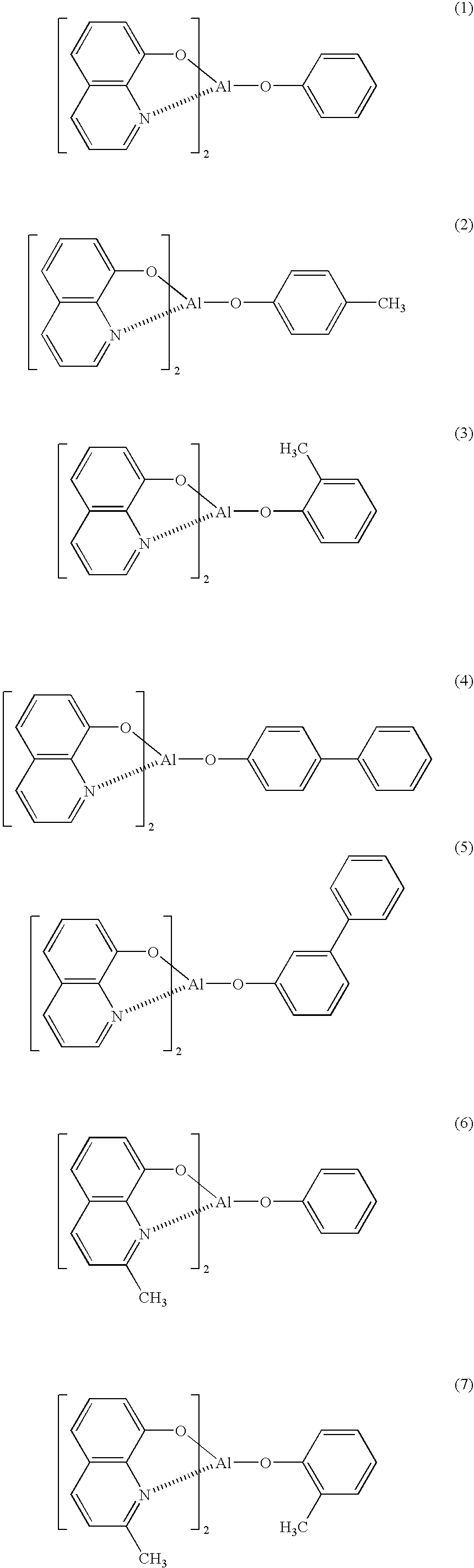
Organic electroluminescence device
a technology of electroluminescence device and organic el, which is applied in the direction of discharge tube luminescence screen, other domestic articles, natural mineral layered products, etc., can solve the problems of deteriorating driving durability, affecting the practical use of organic el devices, and affecting the quality of continuous driving of these devices, so as to improve luminescent efficiency and durability, the effect of reducing the driving voltag
- Summary
- Abstract
- Description
- Claims
- Application Information
AI Technical Summary
Benefits of technology
Problems solved by technology
Method used
Image

Examples
example 1
[0189]1. Production of an Organic EL Device
[0190]>
[0191]An ITO glass substrate (manufactured by Geomatic (k.k.), surface resistance: 10 Ω / □) which had a thickness of 0.5 mm and was 2.5 by 2.5 cm square was placed in a washing container and subjected to ultrasonic cleaning in 2-propanol and then to UV-ozone treatment carried out for 30 minutes. The following layers were vapor deposited on this transparent anode by a vacuum vapor deposition method. The vapor deposition speed in the following examples of the present invention is 0.2 nm / sec unless otherwise noted. The vapor deposition speed was measured using a quarts resonator. The film thicknesses mentioned below were also measured using the quartz resonator.
[0192](Hole Injection Layer)
[0193]2-TNATA and F4-TCNQ (tetrafluorotetracyanoquinodimethane) were co-deposited such that the deposition rate of 2-TNATA was 0.5 nm / sec and the amount of F4-TCNQ was 0.3% by weight based on 2-TNATA. The film thickness was designed to be 55 nm.
[0194](H...
PUM
| Property | Measurement | Unit |
|---|---|---|
| electron mobility | aaaaa | aaaaa |
| thickness | aaaaa | aaaaa |
| thickness | aaaaa | aaaaa |
Abstract
Description
Claims
Application Information