Floating-body DRAM in tri-gate technology

a tri-gate, floating-body technology, applied in the direction of semiconductor devices, electrical apparatus, transistors, etc., can solve the problems of limiting manufacturing costs, limited area used by six transistor (6t) sram cells, and typically used in large caches

Inactive Publication Date: 2006-01-19
INTEL CORP
View PDF2 Cites 234 Cited by
  • Summary
  • Abstract
  • Description
  • Claims
  • Application Information

AI Technical Summary

Problems solved by technology

For example, the area used by six transistor (6T) SRAM cells, which are typically used

Method used


Image

  • Floating-body DRAM in tri-gate technology
  • Floating-body DRAM in tri-gate technology
  • Floating-body DRAM in tri-gate technology

Examples


Embodiment Construction

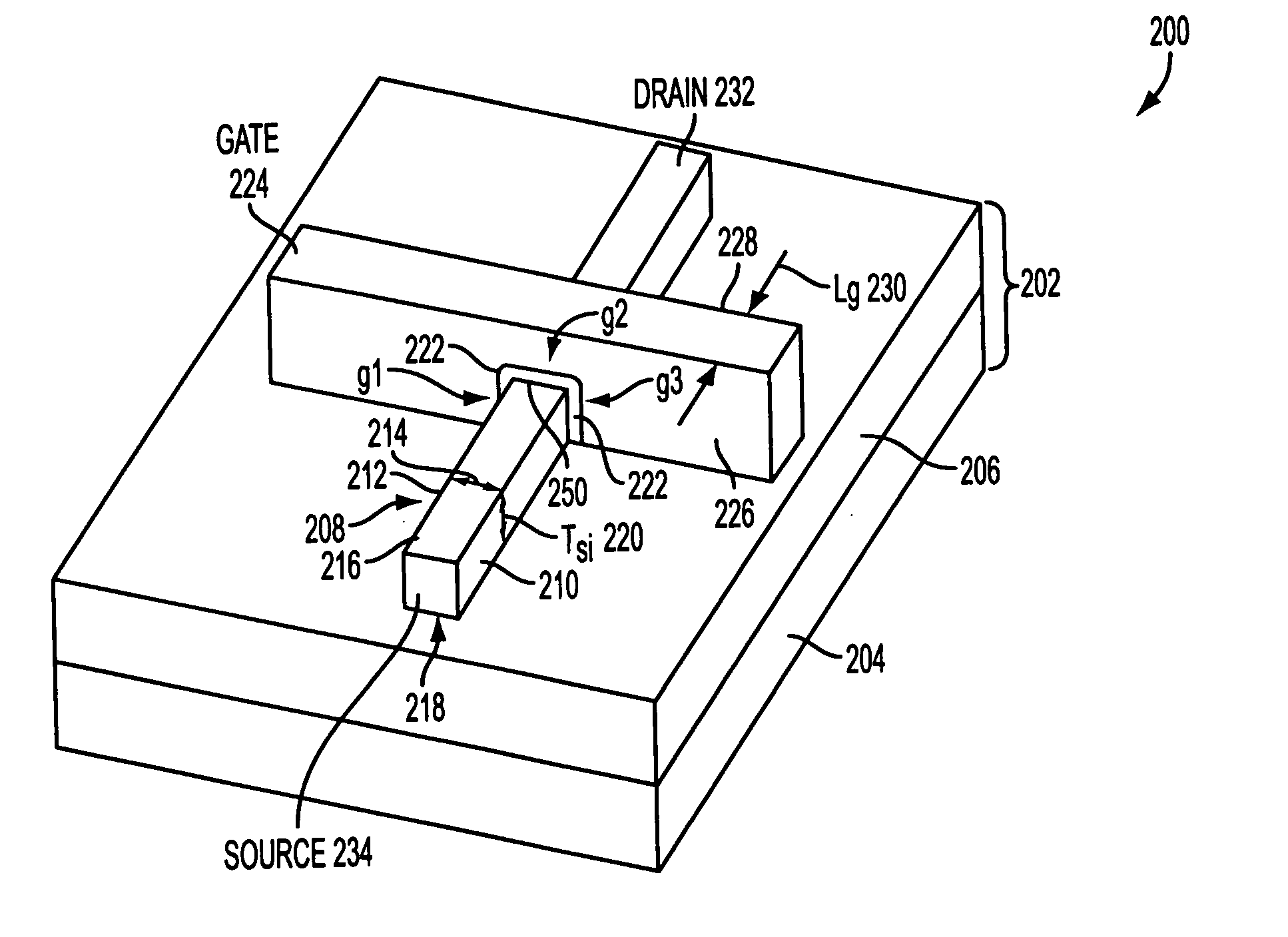
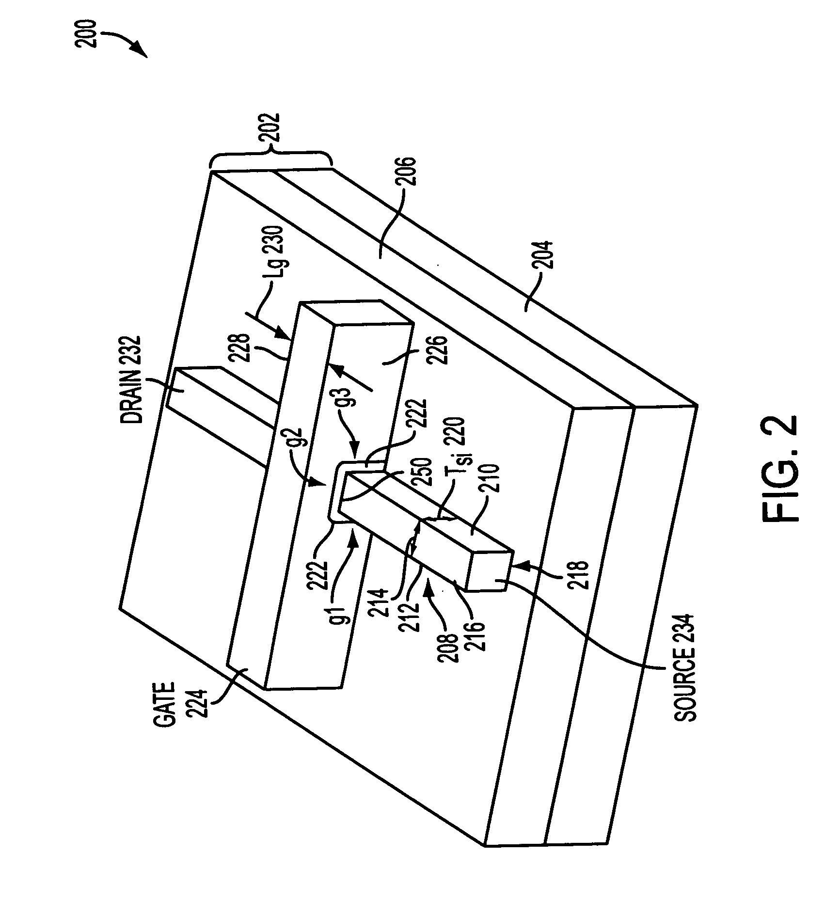
[0013] One embodiment of the invention is a novel floating-body DRAM (FBDRAM) in a tri-gate transistor structure and its method of fabrication. In the following description numerous specific details are set forth in order to provide a thorough understanding in the present invention. In other instances, well-known semiconductor process and manufacturing techniques have not been described in particular detail in order to not unnecessarily obscure the invention.

[0014] In an embodiment of the present invention, the FBDRAM may be implemented in a semiconductor on insulator (SOI) transistor. The FBDRAM may be used in partially depleted substrate transistor applications. In an embodiment of the present invention, the FBDRAM is configured using tri-gate technology that may include a thin semiconductor body formed on a substrate. The substrate may be an insulating substrate or a semiconductor substrate. A gate dielectric may be formed on the top surface and the sidewalls of the semiconducto...


PUM


Abstract

A floating-body dynamic random access memory device may include a semiconductor body having a top surface and laterally opposite sidewalls formed on a substrate. A gate dielectric layer may be formed on the top surface of the semiconductor body and on the laterally opposite sidewalls of the semiconductor body. A gate electrode may be formed on the gate dielectric on the top surface of the semiconductor body and adjacent to the gate dielectric on the laterally opposite sidewalls of the semiconductor body. The gate electrode may only partially deplete a region of the semiconductor body, and the partially depleted region may be used as a storage node for logic states.

Description

BACKGROUND OF THE INVENTION [0001] Efforts to integrate more on-die memory, that is, larger caches, with a microprocessor are guided by the premise that to do so is a power-efficient means of achieving better performance. For example, the area used by six transistor (6T) SRAM cells, which are typically used in large caches, is limited by constraints on die size and to limit manufacturing costs. Thus, a key to enabling larger caches is minimizing the additional cost of incorporating a denser memory cell than SRAM. [0002] One transistor—One Capacitor (1T-1C) DRAM cells have been proposed. These DRAM cells strive to be ten times smaller in area than traditional SRAM cells. The design goals for these DRAM cells need to account for the greater costs involved in making a capacitor that can store enough charge to maintain reasonable refresh times. For example, capacitances at least of 25 fF are calculated to be required. [0003] The recent work in DRAM gain cells has sought to fabricate cel...

Claims


Application Information

Patent Timeline
IPC IPC(8): H01L21/84
CPCH01L27/108H01L27/10802H01L27/10826H01L29/785H01L27/10879H01L29/66795H01L29/7841H01L27/10876H10B12/20H10B12/36H10B12/056H10B12/053H10B12/00
Inventor TANG, STEPHEN H.KESHAVARZI, ALISOMASEKHAR, DINESHPAILLET, FABRICEKHELLAH, MUHAMMAD M.YE, YIBINLU, SHIH-LIEN L.DOYLE, BRIANDATTA, SUMANDE, VIVEK K.
Owner INTEL CORP
Why Eureka
Try Eureka