Electron beam apparatus

a technology of electron beam and apparatus, which is applied in the direction of instruments, nuclear engineering, heat measurement, etc., can solve the problems of degradation in resolution, difficult mechanical shifting of stage, and unnegligible problem of degradation in resolution

Inactive Publication Date: 2006-01-26
HITACHI LTD
View PDF5 Cites 10 Cited by
  • Summary
  • Abstract
  • Description
  • Claims
  • Application Information

AI Technical Summary

Benefits of technology

[0007] An object of the present invention is to provide an electron beam apparatus suitable for performing image shift in an arbitrary direction without degrading the resolution.

Problems solved by technology

However, because the mechanical shifting of the stage becomes difficult when the magnification of observation is high, image shift is used in order to shift a field of observation view to the observation center.
However, when image shift is performed, the primary electron beam is energy-dispersed corresponding to the amount of image shift in the shift direction to cause degradation in the resolution.
The degradation in the resolution becomes an un-negligible problem as the resolution of the apparatus is increased.

Method used


Image

  • Electron beam apparatus
  • Electron beam apparatus
  • Electron beam apparatus

Examples


Embodiment Construction

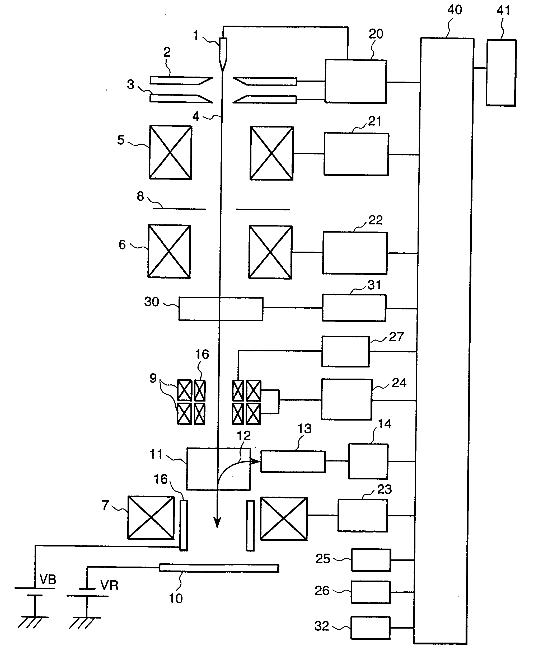
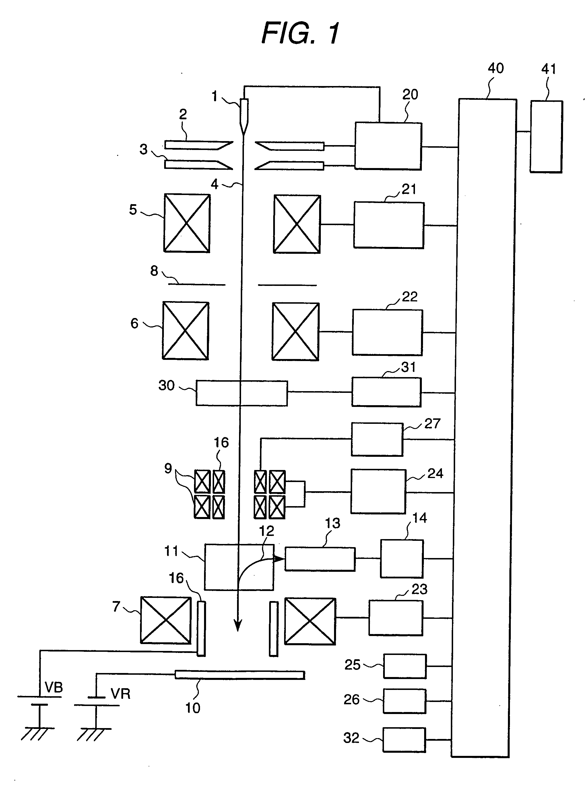
[0021] An electron beam emitted from an electron source has deviation in energy due to characteristics of the electron source. For example, an electron beam emitted from an electron source of a Schottky type obtainable of a high bright electron beam has an energy width of 0.4 eV to 0.6 eV. When the electron beam having such energy deviation is electrically deflected, the electron beam reaching a sample is energy dispersed corresponding to the deviation in energy because the amount of deflection depends on the energy of the beam. Since the energy dispersion causes a blur of the electron beam, the resolution is degraded. Before describing concrete embodiments of the present invention, the principle of the degradation of resolution will be described first.

[0022] Referring to FIG. 7, the primary electron beam 4 is deflected by a magnetic field produced by a deflection coil 15 to be irradiated onto a sample 10 through a center of an objective lens 7. Letting a deflected amount on the sa...


PUM

PropertyMeasurementUnit
energy widthaaaaaaaaaa
acceleration voltageaaaaaaaaaa

Abstract

An electron beam (4) to be irradiated onto a sample (10) is two-dimensionally scanned by a scanning coil (9), and secondary electrons generated from the sample (10) by the scanning are detected by a secondary electron detector (13). A deflection coil (15) for image shifting is used for electrically deflecting the primary electron beam to shift a field of view for image shift in an arbitrary direction by an arbitrary amount. By the image shift, the primary electron beam (4) to be irradiated onto the sample is energy dispersed to degrade the resolution. However, an E×B field producer (30) for dispersion control gives the primary electron beam energy dispersion in the opposite direction and having the equal magnitude. Therefore, the energy dispersion produced in the primary electron beam by the image shift is automatically corrected.

Description

TECHNICAL FIELD [0001] The present invention relates to an electron beam apparatus, and particularly to an electron beam apparatus such as a scanning electron microscope for performing evaluation of a micropattern in a semiconductor device or general-purpose observation of a general sample. BACKGROUND ART [0002] An electron beam apparatus such as a scanning electron microscope obtaining a scanning image of a sample by scanning a primary electron beam on the sample is used for a purpose of pattern evaluation such as inspection or measurement of a micropattern in a semiconductor device. The apparatus of such a kind comprises an image shift function for electrically shifting an electron beam irradiation area (a field of observation view) within a range of several μm to 10 μm by electrically deflecting the primary electron beam in order to shift the field of observation view to an evaluation point with high accuracy. [0003] On the other hand, in a scanning electron microscope used for a...

Claims


Application Information

Patent Timeline
Patent Type & Authority Applications(United States)
IPC IPC(8): G21K7/00G01N23/00G01Q30/02H01J37/05H01J37/147H01J37/153H01J37/28
CPCH01J37/05H01J37/1474H01J2237/2817H01J2237/1536H01J37/153H01J37/147
Inventor SATO, MITSUGUTODOKORO, HIDEO
Owner HITACHI LTD
Why Eureka
Try Eureka