Structure and formation method of conductive bumps

Inactive Publication Date: 2006-01-26
ADVANCED SEMICON ENG INC
View PDF11 Cites 49 Cited by
  • Summary
  • Abstract
  • Description
  • Claims
  • Application Information

AI Technical Summary

Benefits of technology

[0007] It is one of objectives of the present invention to provide a conductive bump herein for preventing nickel elements from diffusing into a wetting layer. With the addition of a conductive barrier layer between the solder ball and the wetting layer would block the diffusion of the nickel elements.
[0008] It is another one of objectives of the present invention to provide a conductive bump with a cup structure of adhesion / diffusion barrier layer to prevent the nickel elements from diffusing through the UBM layer.
[0009] It is still another one of objectives of the present invention to provide the formation method of conductive bumps. An adhesion / diffusion barrier with a side wall would prevent the nickel elements from diffusing through the side wall of the UBM for fear of the formation of the excess IMC.

Problems solved by technology

An issue on solder balls is derived from a reflow process.
Furthermore, the heavy consumption of the nickel elements of the solder ball 22 makes the solder ball 22 with little area connect with a printed circuit board and further the poor connection during sequential processes.

Method used


Image

  • Structure and formation method of conductive bumps
  • Structure and formation method of conductive bumps
  • Structure and formation method of conductive bumps

Examples


Embodiment Construction

[0014] The following description is of the best presently contemplated mode of carrying out the present invention. This description is not to be taken in a limiting sense but is made merely for the purpose of describing the general principles of the invention. The scope of the invention should be determined by referencing the appended claims.

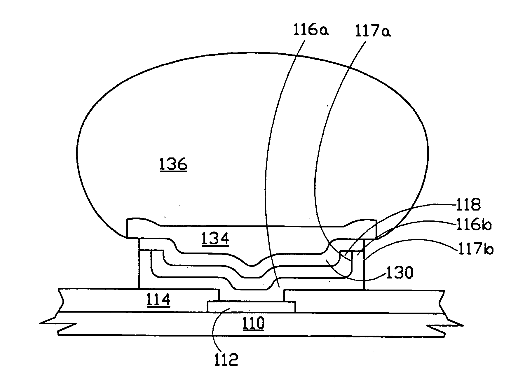
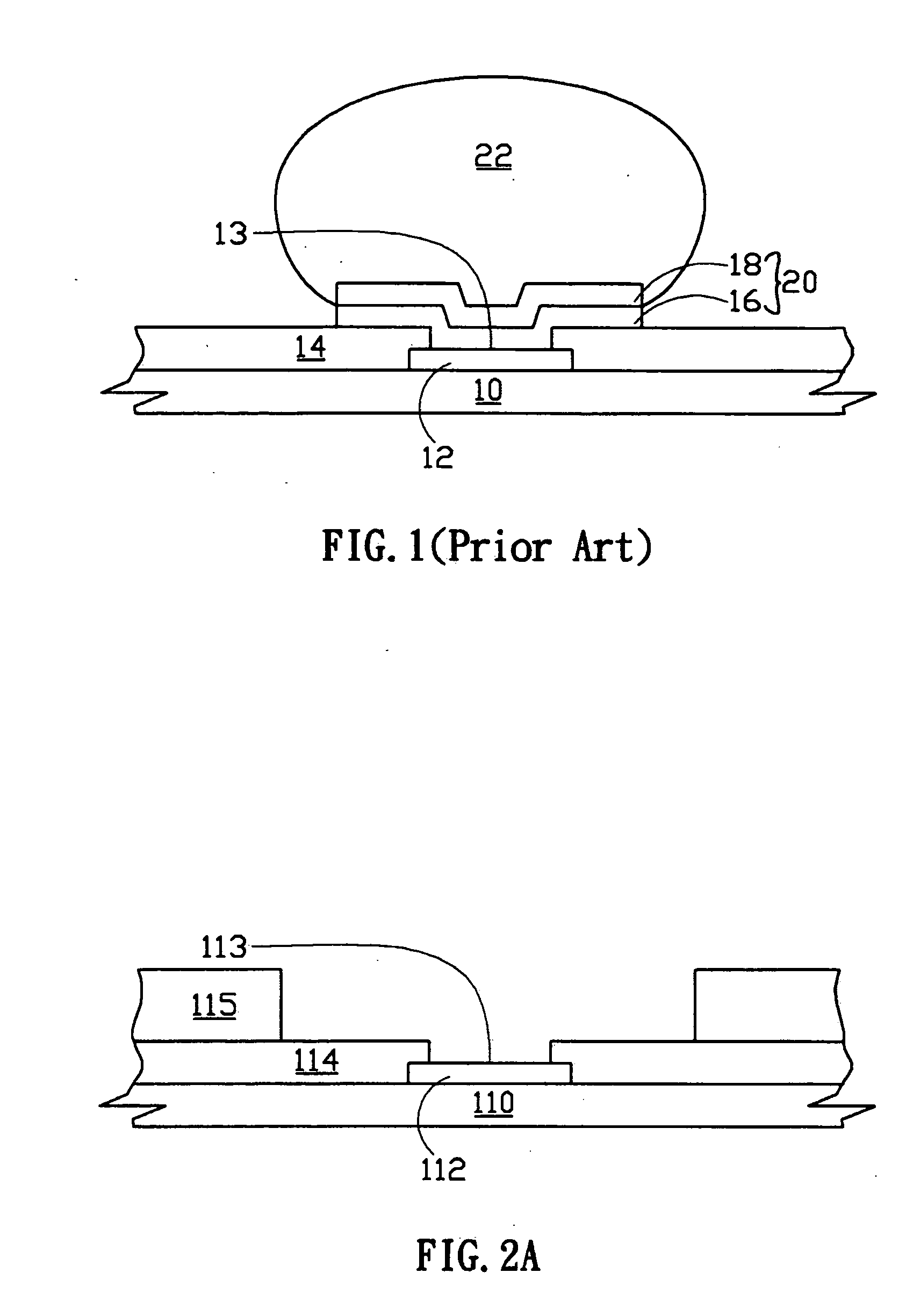
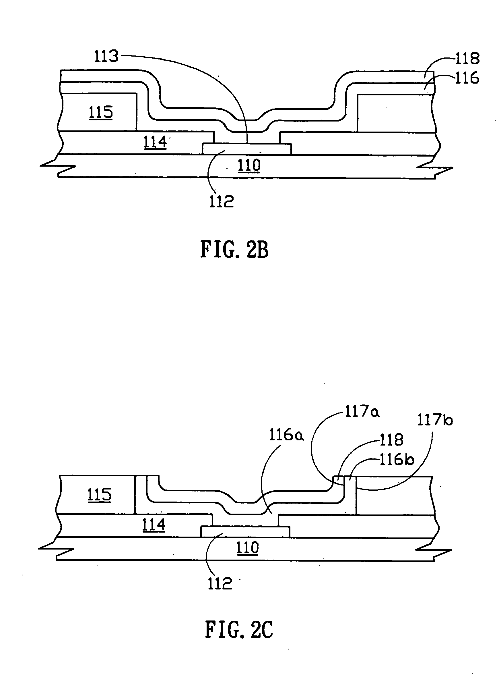
[0015] A conductive bump structure and the formation are provided herein. A conductive surface is provided on a wafer. The under bump metallurgy layer is formed on the conductive surface. The under bump metallurgy layer has a first conductive barrier layer, a conductive wetting layer, a conductive seed layer and a second conductive barrier layer. The first conductive barrier layer is in a cup shape and with a bottom attaching the conductive surface and a peripheral flange. The conductive wetting layer covers the bottom and an inside side wall of the peripheral flange. The conductive wetting layer and the peripheral flange reach up a same top su...


PUM


Abstract

A method and structure for a conductive bump are provided herein. A conductive surface is provided on a wafer. A conductive barrier layer and a conductive wetting layer on a part of the conductive surface have a bottom and a side wall and further reach up a top surface. The conductive wetting and barrier layers constitute inside and outside side walls, respectively. A conductive seed layer covers the conductive wetting layer and the top surface. Another conductive barrier and conductive bump are subsequently formed on the conductive seed layer.

Description

BACKGROUND OF THE INVENTION [0001] 1. Field of the Invention [0002] The present invention generally relates to a structure and a formation method of conductive bumps and, more particularly to conductive bumps each having an under bump metallurgy layer with a side wall. [0003] 2. Discussion of the Related Art [0004] With the technology of the integrated circuit in development the qualities on the package of the integrated circuit is in demand. Ball Grid Array Package (BGA) is mostly applied to high-pin chips, such as picture chips or chip sets. The substrate types of BGA include various types: Plastic BGA (PBGA), Ceramic BGA (Ceramic BGA), Flip Chip BGA (FCBGA), Tape BGA (TBGA) and Cavity Down PBGA. For example, FCBGA is to assign gold studs or solder bumps on an IC chip for connecting with a print circuit board. [0005] For example, shown in FIG. 1 is a cross-sectional diagram illustrating a solder ball by thin film deposition in accordance with the prior art. Depicted as FIG. 1, a b...

Claims


Application Information

Patent Timeline
IPC IPC(8): H01L21/44H01L23/48H01L23/52H01L21/60H01L23/485
CPCH01L24/02H01L24/11H01L2924/0001H01L2224/13144H01L2224/131H01L2924/01023H01L24/13H01L2224/0401H01L2224/13099H01L2924/01013H01L2924/01014H01L2924/01028H01L2924/01029H01L2924/01073H01L2924/01078H01L2924/01079H01L2924/01327H01L2924/014H01L2924/04953H01L2924/14H01L2924/00014H01L2224/13006H01L2224/05076H01L24/03H01L24/05
Inventor HUANG, MIN-LUNG
Owner ADVANCED SEMICON ENG INC
Why Eureka
Try Eureka