Metal-insulator-metal capacitor and interconnecting structure

Inactive Publication Date: 2005-02-03
SAMSUNG ELECTRONICS CO LTD
View PDF2 Cites 33 Cited by
  • Summary
  • Abstract
  • Description
  • Claims
  • Application Information

AI Technical Summary

Benefits of technology

[0018] Embodiments of the present invention relate to a method of manufacturing a semiconductor device in which a via connecting an interconnecting structure and a via connecting a MIM capacitor are formed at equal depths. Accordingly, in embodiments, the capacitance of the MIM capacitor may be increased and the reliability of the interconnecting structure and the MIM capacitor may be enhanced.
[0029] In embodiments, the lower metal interconnecting layer and the conductive film are formed of copper. However, in other embodiments, the lower metal interconnecting layer and the conductive film can be formed of a material selected from a group consisting of Al, Au, Ag, Ti, Ta, W and an alloy of these metals. In embodiments, the barrier metal layers are formed of a layer selected from a group of consisting of a Ta layer, a TaN layer, a WN layer, and a layer with a Ta layer / TaN layer structure. The barrier layers may block the diffusion of the conductive film into the inter-metal insulating film.

Problems solved by technology

However, a metal-insulator-semiconductor (MIS) capacitor may have the drawback of low capacitance due to a low dielectric constant film between a polysilicon film and a dielectric film.
However, copper interconnecting patterns are generally not formed by an etching process.
Rather, copper interconnecting patterns may be formed by a damascene process, because copper can be a difficult material to etch.
In forming an interconnecting structure and an MIM capacitor using a damascene process, difficulty may be encountered in manufacturing vias due to the different depths of vias in the interconnecting structure and the MIM capacitor.
Accordingly, the metal electrode under the via may be damaged due to different etching depths.
However, in this method (of Korean Laid-Open Patent publication 2000-53453), since a portion (for forming the trench of the MIM capacitor) is masked while depositing metal to form a interconnecting structure using a photoresist mask, a selective metal deposition is practically impossible.
However, photoresist material may be degraded by the sulfuric acid solution.
Therefore, the photoresist material for masking the trench portion cannot perform an adequate masking role.
The process may be necessarily complicated, because electroplating the interconnecting structure and electroplating the MIM capacitor must be performed separately.
Planarization of a copper layer after electroplating may also be difficult, due to the large step.

Method used


Image

  • Metal-insulator-metal capacitor and interconnecting structure
  • Metal-insulator-metal capacitor and interconnecting structure
  • Metal-insulator-metal capacitor and interconnecting structure

Examples


example

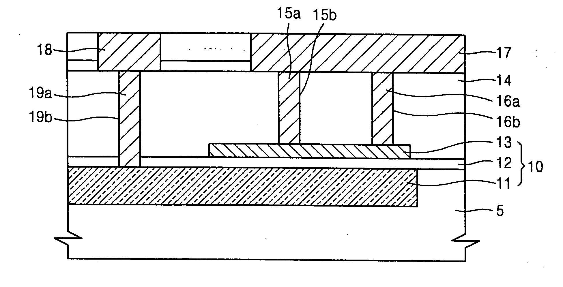
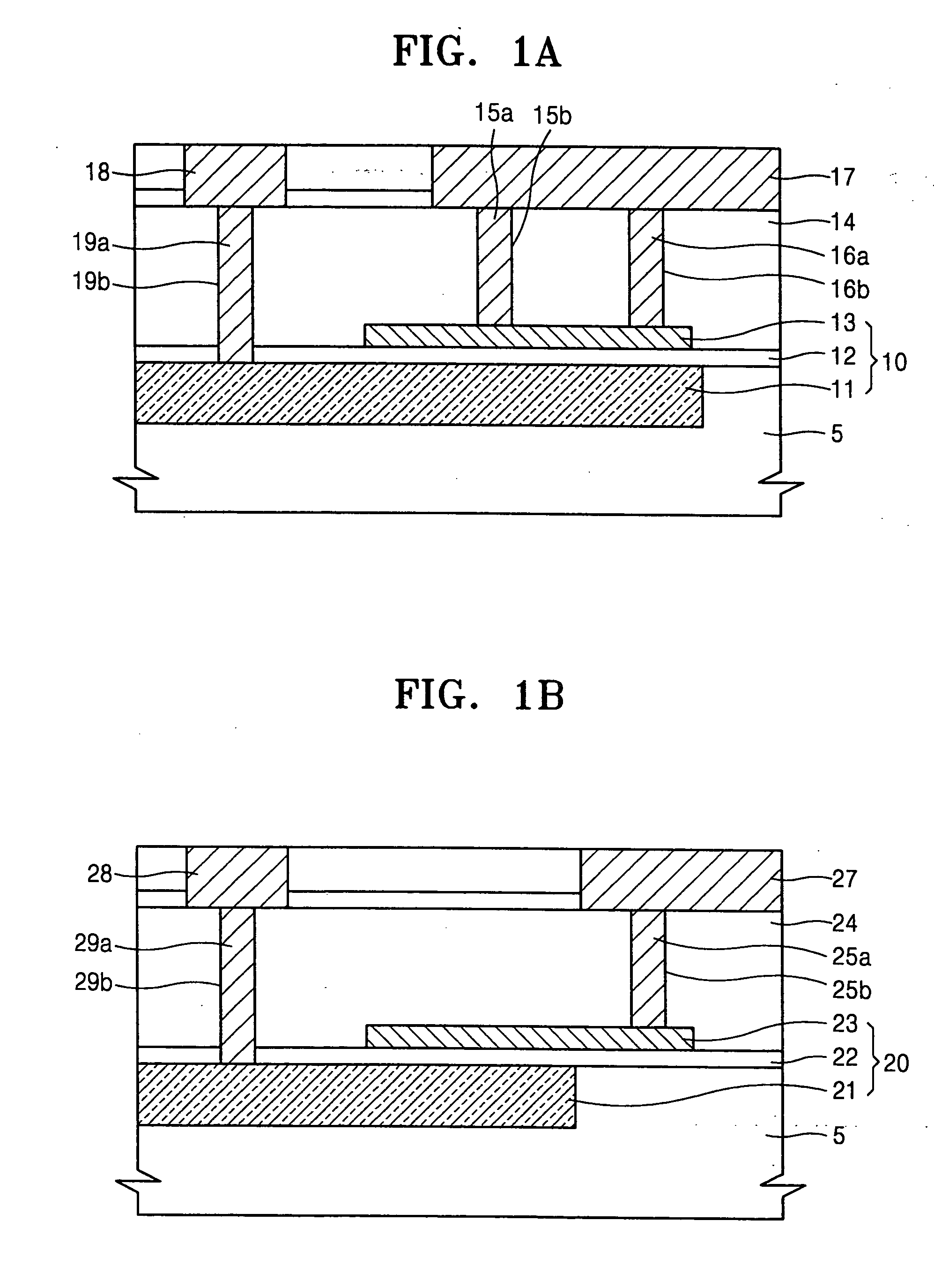
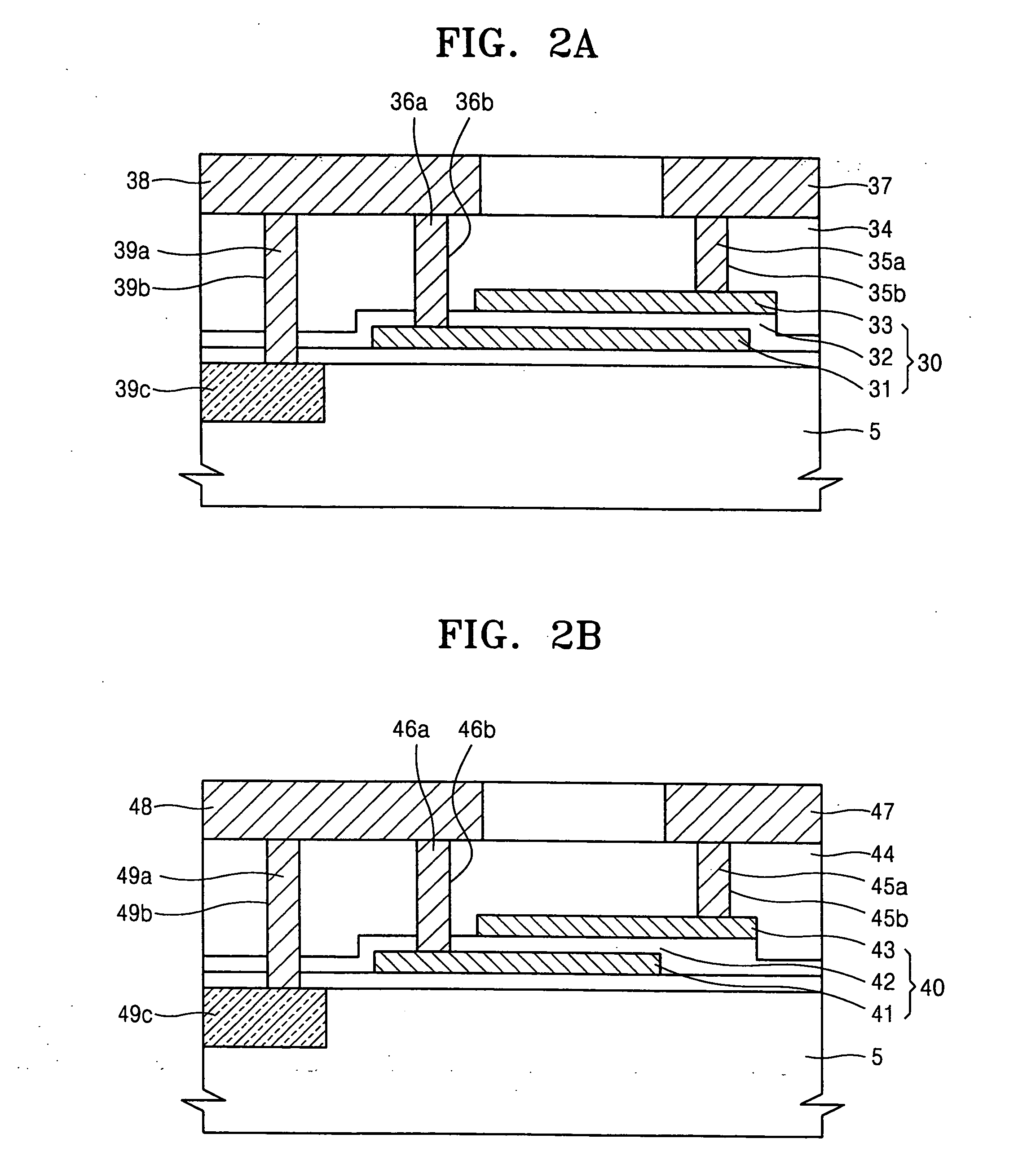
[0051] Example FIGS. 17 through 29 are cross-sectional views according to embodiments of the present invention. In embodiments, a via for metal interconnecting having the same depth as a trench for an MIM capacitor is formed at the same time as the trench for the MIM capacitor.

[0052] Referring to example FIG. 17, a lower metal interconnecting layer 60 (e.g. formed of copper) is formed in an insulating film 50 on a semiconductor substrate (not shown). Thin etch stoppers 201 and 203 formed of SiC, SiN, SiCN, or SiCO are formed on the lower metal interconnecting layer 60 and between the inter-metal insulating films 202 and 204. A buffer insulating film 71 (e.g. formed of FSG or USG) is formed on the inter-metal insulating film 204. A photo-resist pattern 81 is formed on the buffer insulating film 71 to form a trench for the MIM capacitor and a via for a metal interconnecting.

[0053] Referring to example FIG. 18, a trench 251 for the MIM capacitor and a via 261 for the metal interconnec...


PUM


Abstract

A method of manufacturing a MIM capacitor and a interconnecting structure using a damascene process. The MIM capacitor and the first interconnecting structure can be formed at equal depths.

Description

BACKGROUND OF THE INVENTION [0001] 1. Field of the Invention [0002] Embodiments of the present invention relate to manufacturing a semiconductor device including a capacitor (e.g. MIM capacitor) and interconnecting structure using a damascene process. [0003] This application claims the priority of Korean Patent Application No. 2003-52398 filed on Jul. 29, 2003, in the Korean Intellectual Property Office, the disclosure of which is incorporated herein in its entirety by reference. [0004] 2. Description of the Related Art [0005] As the integration density of semiconductor devices increases in certain applications, increased capacitance of capacitors is required to ensure safe operation of the capacitors. However, a metal-insulator-semiconductor (MIS) capacitor may have the drawback of low capacitance due to a low dielectric constant film between a polysilicon film and a dielectric film. Therefore, a metal-insulator-metal (MIM) capacitor may be used for safer operation. [0006] A MIM ca...

Claims


Application Information

Patent Timeline
IPC IPC(8): G11C8/02H01L21/768H01L21/02H01L21/822H01L21/8242H01L27/04
CPCH01L28/75H01L28/40H10B99/00
Inventor KIM, YOON-HAELEE, KYUNG-TAELIU, SEONG-HO
Owner SAMSUNG ELECTRONICS CO LTD
Why Eureka
Try Eureka