Forming a plurality of thin-film devices
a thin-film device and film technology, applied in the field of semiconductor devices, can solve the problems of putting a larger burden on the mask mastering, etching and imprinting process
- Summary
- Abstract
- Description
- Claims
- Application Information
AI Technical Summary
Problems solved by technology
Method used
Image

Examples
Embodiment Construction
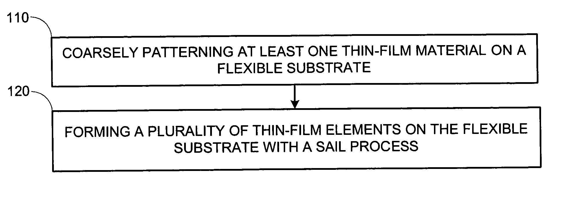
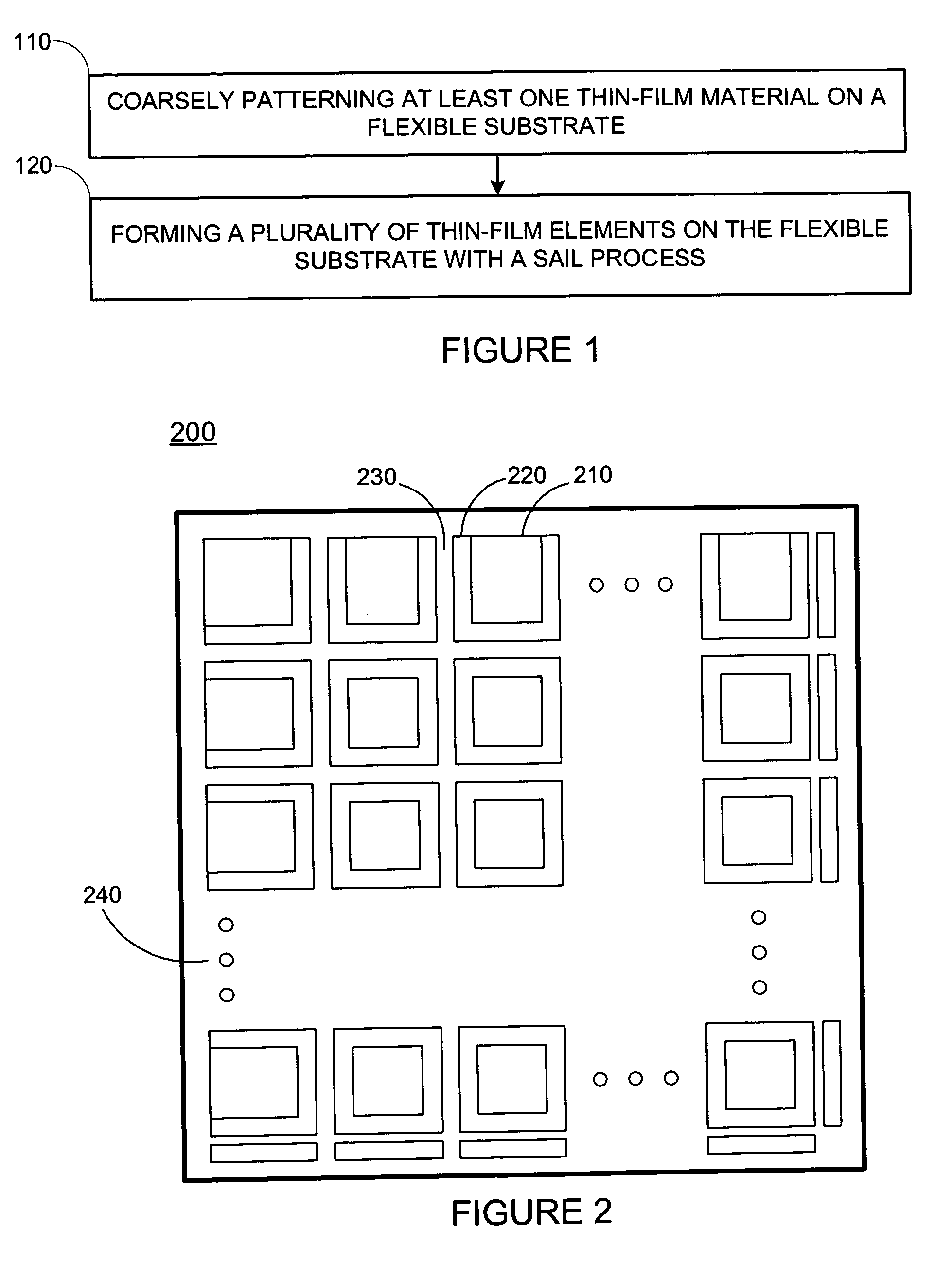
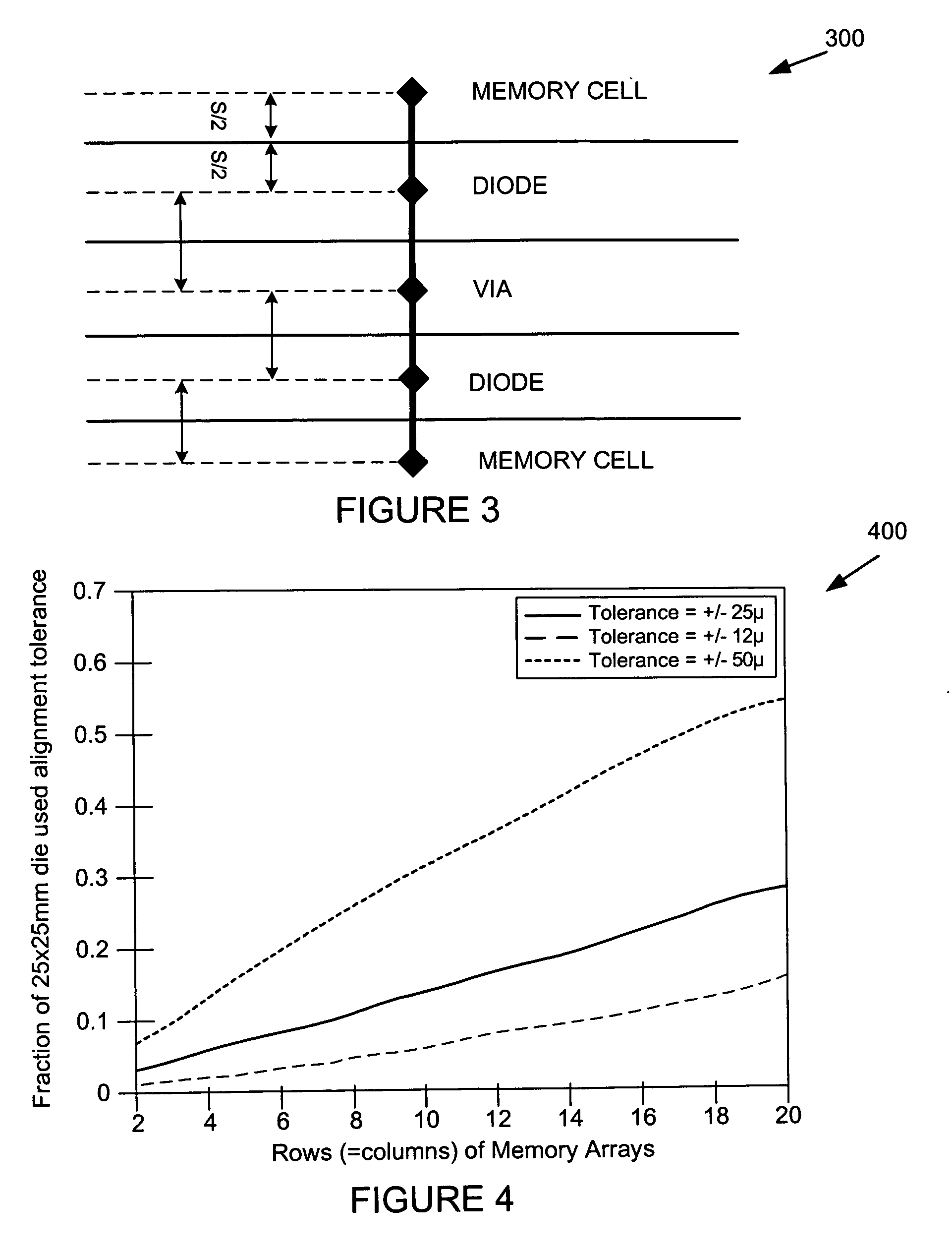
[0020] The present invention relates to a method and system for forming a plurality of thin-film elements. The following description is presented to enable one of ordinary skill in the art to make and use the invention and is provided in the context of a patent application and its requirements. Various modifications to the embodiments and the generic principles and features described herein will be readily apparent to those skilled in the art. Thus, the present invention is not intended to be limited to the embodiment shown but is to be accorded the widest scope consistent with the principles and features described herein.
[0021] As shown in the drawings for purposes of illustration, a method and system for forming a semiconductor device is disclosed. Varying embodiments of the method and system provide a coarse patterning step to be utilized in conjunction with a self-aligned imprint lithography (SAIL) process in order to form a plurality of thin-film elements on a flexible substra...
PUM
| Property | Measurement | Unit |
|---|---|---|
| Structure | aaaaa | aaaaa |
| Flexibility | aaaaa | aaaaa |
| Height | aaaaa | aaaaa |
Abstract
Description
Claims
Application Information
 - Generate Ideas
- Intellectual Property
- Life Sciences
- Materials
- Tech Scout
- Unparalleled Data Quality
- Higher Quality Content
- 60% Fewer Hallucinations
Browse by: Latest US Patents, China's latest patents, Technical Efficacy Thesaurus, Application Domain, Technology Topic, Popular Technical Reports.
© 2025 PatSnap. All rights reserved.Legal|Privacy policy|Modern Slavery Act Transparency Statement|Sitemap|About US| Contact US: help@patsnap.com