

Semiconductor device and method for manufacturing the same
a technology of semiconductors and semiconductors, applied in the direction of inductances, galvano-magnetic devices, basic electric elements, etc., can solve the problems of significant influence of parasitic capacitance, energy loss, and part of electromagnetic energy generated by induction elements in the substrate, and achieve low energy-loss and high performance.
Inactive Publication Date: 2006-02-02
FLIPCHIP INT
View PDF6 Cites 31 Cited by
- Summary
- Abstract
- Description
- Claims
- Application Information
AI Technical Summary
Benefits of technology
[0032] The present invention was conceived in light of the above-described background, and one object thereof is to
Problems solved by technology
In such a semiconductor element, however, a part of electromagnetic energy generated by the induction element is lost in the substrate or a wiring constructing the induction element due to parasitic capacitance between the wiring and the semiconductor substrate.
One cause of this type of electromagnetic energy loss is a relatively close vertical distance between the wiring and the semiconductor substrate, which makes the influence of the parasitic capacitance significant.
(1) Because the lower wiring layer 21
Method used
View moreImage
Smart ImageViewing Examples

Examples
 PUM
| Property | Measurement | Unit |
|---|---|---|
| Length | aaaaa | aaaaa |
| Length | aaaaa | aaaaa |
| Width | aaaaa | aaaaa |
Abstract
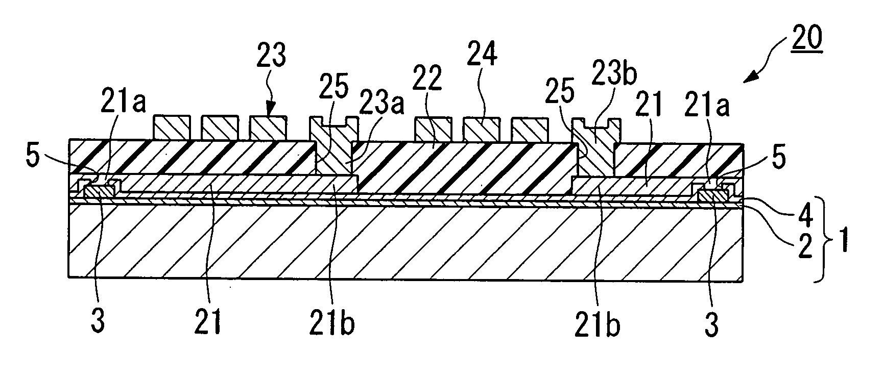
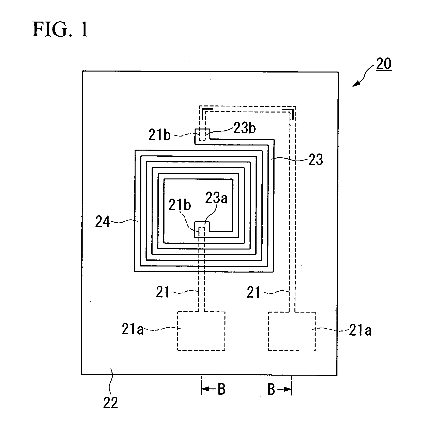
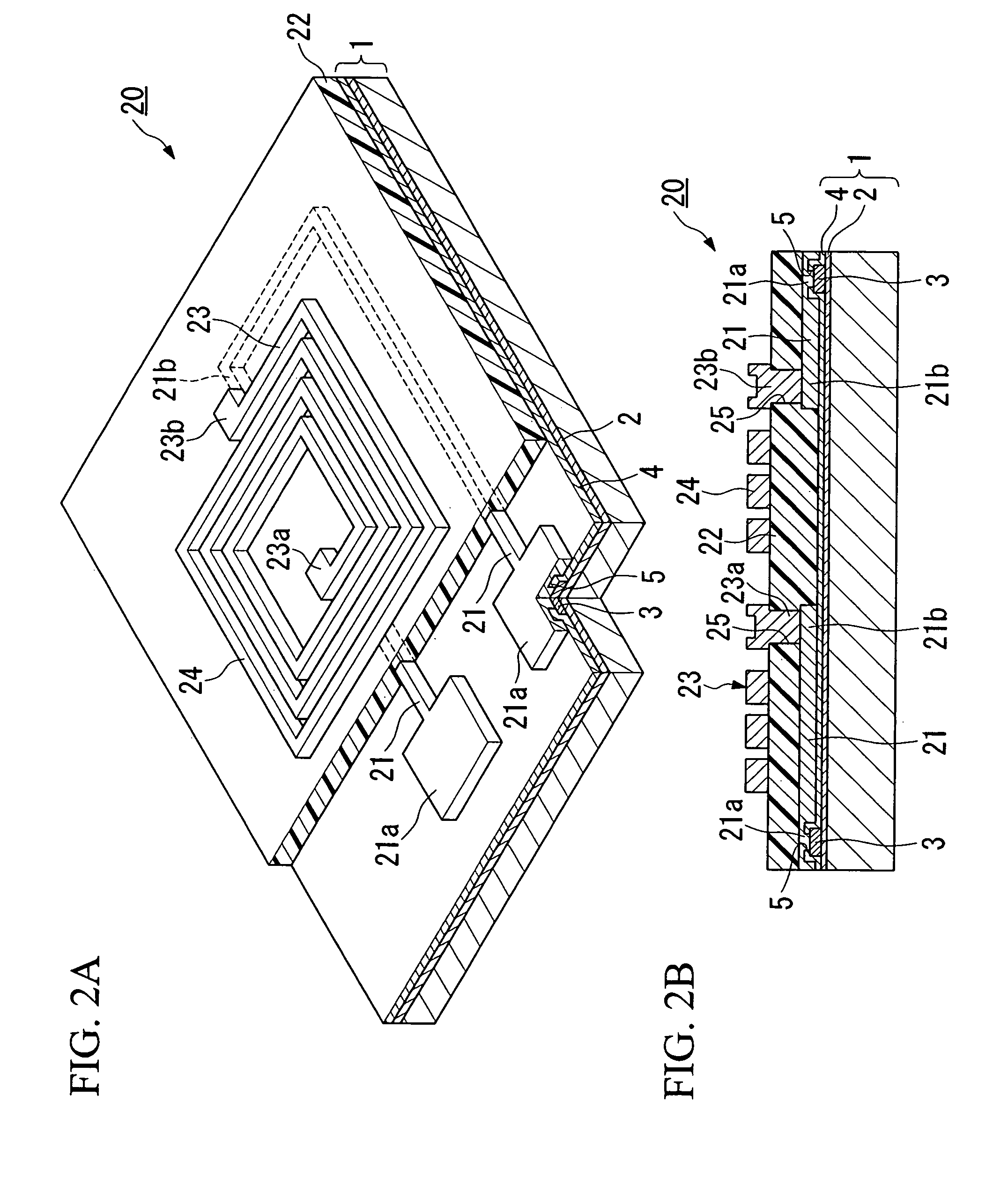
A semiconductor device includes a semiconductor substrate having an electrode formed above a surface thereof; a first insulating resin layer that is provided over the semiconductor substrate and has a first opening defined at a position corresponding to the electrode; a first wiring layer that is provided on the first insulating resin layer and is connected to the electrode through the first opening; a second insulating resin layer provided over the first insulating resin layer and the first wiring layer, the second insulating resin layer having a second opening that is defined at a position different from the position of the first opening in a direction of the surface of the semiconductor substrate; and a second wiring layer that is provided on the second insulating resin layer and is connected to the first wiring layer through the second opening, wherein the second wiring layer includes an induction element, and a sum of a thickness of the first insulating resin layer and a thickness of the second insulating resin layer is not less than 5 μm and not more than 60 μm.
Description
BACKGROUND OF THE INVENTION [0001] 1. Field of the Invention [0002] The present invention relates to a semiconductor device and a method for manufacturing the same in which formation of a semiconductor having a induction element formed above a semiconductor substrate, such as a silicon wafer is done together with packaging thereof. [0003] Priority is claimed on Japanese Patent Application No. 2004-221785, filed Jul. 29, 2004, and Japanese Patent Application No. 2004-302696, filed Oct. 18, 2004, the contents of which are incorporated herein by reference. [0004] 2. Description of Related Art [0005] In recent years, in a fabrication of a high-frequency semiconductor element, an induction element, such as a spiral inductor, is formed on a semiconductor substrate for the purpose of ensuring impedance matching thereof or the like. In such a semiconductor element, however, a part of electromagnetic energy generated by the induction element is lost in the substrate or a wiring constructing ...
Claims
Login to View More Application Information
Patent Timeline
 IPC IPC(8): H01L43/00
CPCY10T29/49117H01L28/10H01L21/822H01L27/04
InventorITOI, KAZUHISASATO, MASAKAZUITO, TATSUYA
OwnerFLIPCHIP INT