Transmission lines and components with wavelength reduction and shielding

a transmission line and wavelength reduction technology, applied in the direction of optics, instruments, light guides, etc., can solve the problems of reducing performance, pulse dispersion and attenuation of the signal being transferred, and limiting the speed and frequency range of the circuit at rf and higher operating frequencies, so as to reduce the chip area of interconnect structures, reduce the loss caused by electric coupling to a substrate, and reduce the effect of energy loss to the substra

Inactive Publication Date: 2005-09-27
CHEUNG TAK SHUN +1
View PDF7 Cites 63 Cited by
  • Summary
  • Abstract
  • Description
  • Claims
  • Application Information

AI Technical Summary

Benefits of technology

[0010]In another aspect, there is provided a slow-wave transmission line component having a slow-wave structure. The slow-wave structure includes a floating shield employing one of electric and magnetic induction to set a potential on floating strips of said floating shield to about 0, thereby reducing losses caused by electric coupling to a substrate.
[0011]Advantageously, the present invention provides novel transmission lines with reduced energy loss to the substrate and reduced chip area for interconnect structures with a given wavelength on-chip, compared to conventional microstrip and coplanar waveguide transmission lines. In one particular transmission line according to an aspect of the present invention, wavelength reduction achieves a Q-factor>20 from 25 to 40 GHz, or about three times higher than conventional (MIM) transmission lines implemented with the same technology. An approximate loss of 0.3 dB / mm results, with the wavelength reduced by about a factor of two compared to a conventional transmission, thereby minimizing the chip area consumed by on-chip microwave devices.

Problems solved by technology

Shrinking transistor dimensions on-chip have increased gain-bandwidth frequencies beyond 200 GHz, however, it is widely recognized that passive components now limit the speed and frequency range of circuits at RF and higher operating frequencies.
While this transmission line is simple, it suffers from high energy dissipation into the semiconducting silicon material resulting in pulse dispersion and attenuation of the signal being transferred that increases with increasing frequency.
Leakage of the electromagnetic fields via the slots to the underlying semiconductor, and dissipation due to current flow in the metals cause losses resulting in decreased performance.
These losses are, however, substantially lower than for the MISM or CPW transmission lines.

Method used


Image

  • Transmission lines and components with wavelength reduction and shielding
  • Transmission lines and components with wavelength reduction and shielding
  • Transmission lines and components with wavelength reduction and shielding

Examples


second embodiment

[0047]Reference is made to FIG. 9 to describe a transmission line of the present invention. FIG. 9 shows a top view of a portion of a balanced or differential transmission line 220 that includes a pair of coplanar balanced signal conductors 238, 240 and a plurality of metal strips 236 disposed beneath the balanced signal conductors 238, 240. It will be appreciated that the coplanar balanced signal conductors 238, 240 include a positive phase signal conductor 238 and a negative phase signal conductor 240. The metal strips 236 are not connected to either of the signal conductors 238, 240 and inhibit the electric field from radiating to the underlying semiconducting silicon substrate. Again the minimum dimension (or width, as measured in the same direction as current flow in the overlying signal conductors) of the strips 236 is oriented to inhibit current induced via magnetic induction between the top coplanar conductors and the strips. It will now be understood that the signal conduct...

third embodiment

[0048]Reference is now made to FIG. 10 to describe a transmission line of the present invention. FIG. 10 shows top view of a portion of a coupled transmission line 320 that includes a first signal line 342 coupled to a second signal line 344. A plurality of metal strips 336 are disposed beneath the first signal line 342 and a floating shield 346 is disposed beneath the second signal line 344. The plurality of metal strips 336 are not connected to either the first or the second signal lines 342, 344, respectively, and inhibit the electric field from the first signal line 342 from radiating to the semiconducting silicon substrate. Similar to the above-described embodiments, the minimum dimension of the strips 336 is oriented to inhibit current induced between the first signal line 342 and the metal strips 336. It will now be understood that the wavelength of the first signal line 342 is smaller than the wavelength of the second signal line 344. Thus, waves travel at different speeds i...

fourth embodiment

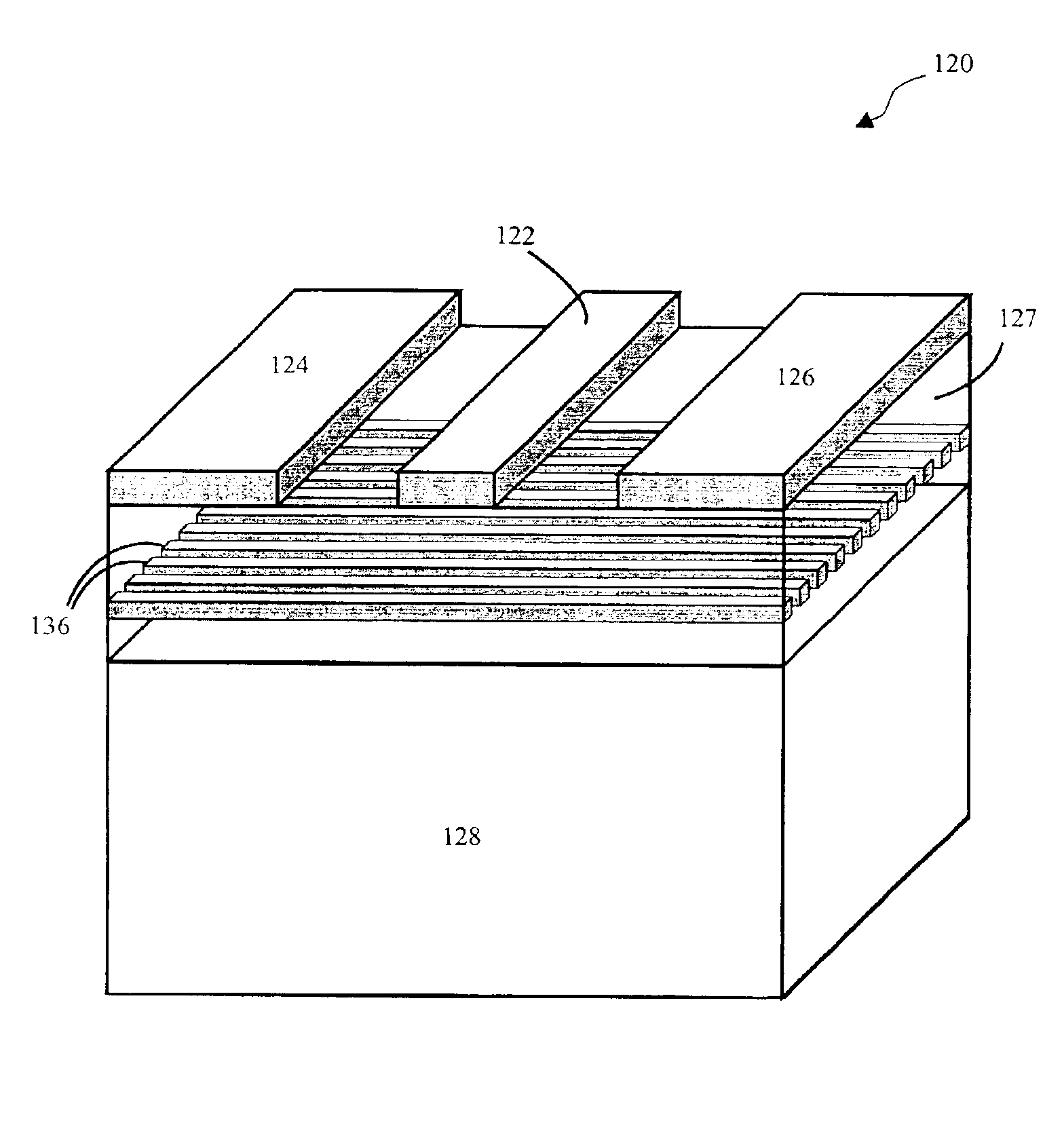
[0049]Reference is made to FIG. 11 to describe the present invention. FIG. 11 shows a top view of a portion of a single ended transmission line 420 that is similar to the first described embodiment and includes three coplanar conductors, a center signal conductor 422 with two adjacent ground strips 424, 426 to form a coplanar waveguide. A plurality of metal strips 436 are disposed beneath the signal conductor and the ground strips. In the present embodiment, however, the metal strips 436 are connected to the ground conductors 424, 426 through electrical vias 448, 450. Thus, in the present embodiment, the metal strips 436 are not “floating strips”, as in the first-described embodiment. This provides a transmission line with reduced wavelength.


PUM


Abstract

A slow-wave transmission line component having a slow-wave structure. The slow-wave structure includes a floating shield employing one of electric and magnetic induction to set a potential on floating strips of said floating shield to about 0, thereby reducing losses caused by electric coupling to a substrate. A spacing between the strips is small to inhibit electric field from passing the metal strips to the substrate material.

Description

FIELD OF THE INVENTION[0001]The present invention relates in general to transmission lines and transmission line components, in particular novel electric shielding of transmission lines and components constructed therefrom.BACKGROUND OF THE INVENTION[0002]Faster, silicon-based technologies are driving new applications such as wireless LAN, point-to-multipoint distribution, and broadband data services such as gigabit per second (Gb / s) fibre-based systems. Shrinking transistor dimensions on-chip have increased gain-bandwidth frequencies beyond 200 GHz, however, it is widely recognized that passive components now limit the speed and frequency range of circuits at RF and higher operating frequencies. Energy coupled to the semiconducting substrate in silicon technologies via passive components is quickly dissipated. This constrains the gain and bandwidth of monolithic circuits. Also, at frequencies where wavelengths are shorter than 10 mm (i.e., millimeter-wave or above 12 GHz for signal...

Claims


Application Information

Patent Timeline
Patent Type & Authority Patents(United States)
IPC IPC(8): H01P3/00
CPCH01P3/003
Inventor CHEUNG, TAK SHUNLONG, JOHN ROBERT
Owner CHEUNG TAK SHUN
Why Eureka
Try Eureka