Dual scan display panel driver

a display panel and driver technology, applied in the field of dual scan display panel drivers, can solve the problems of display function degrade, display is not operating properly,

Inactive Publication Date: 2006-02-02
LAPIS SEMICON CO LTD
View PDF7 Cites 33 Cited by
  • Summary
  • Abstract
  • Description
  • Claims
  • Application Information

AI Technical Summary

Benefits of technology

[0006] When the dual scan system is used, however, if the screen saving function is implemented by the two separate LSI driver circuits, two independent screen saving images are displayed simultaneously in the two halves of the screen, giving the impression that the display is not operating properly.

Problems solved by technology

A disadvantage of organic EL displays is that their display function degrades if the same image is displayed continuously.
When the dual scan system is used, however, if the screen saving function is implemented by the two separate LSI driver circuits, two independent screen saving images are displayed simultaneously in the two halves of the screen, giving the impression that the display is not operating properly.

Method used


Image

  • Dual scan display panel driver
  • Dual scan display panel driver
  • Dual scan display panel driver

Examples


first embodiment

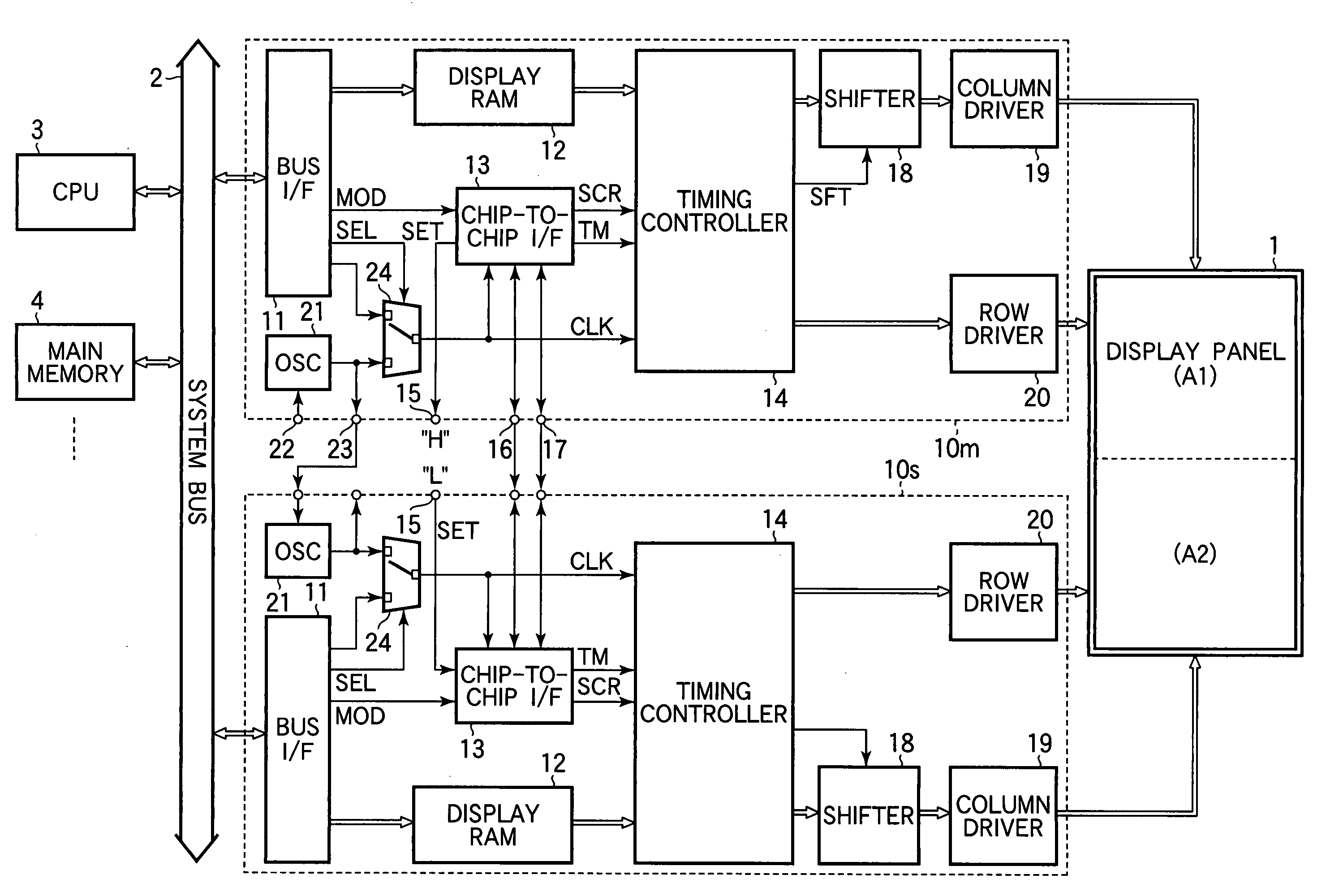
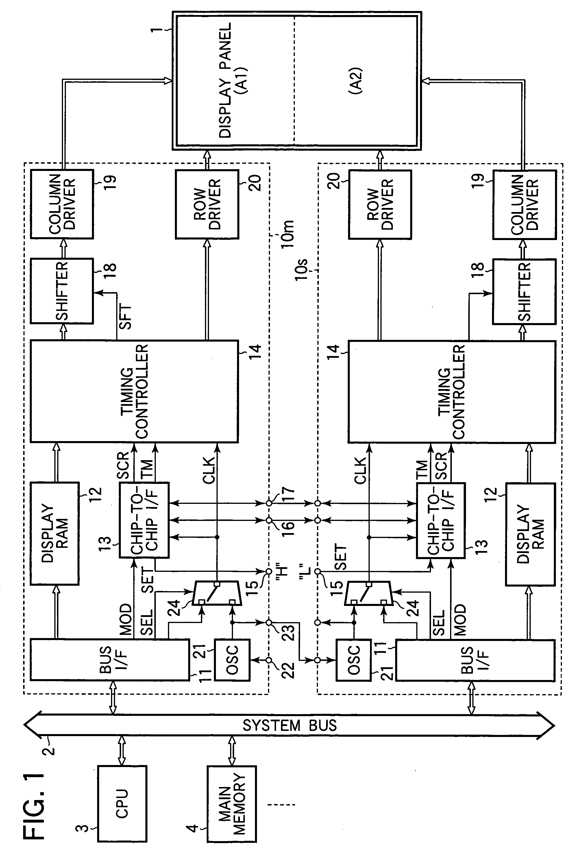
[0016] Referring to FIG. 1, the display panel driver in the first embodiment drives a display panel 1 that is divided vertically into two display areas. A master chip 10m drives the upper display area A1; a slave chip 10s drives the lower display area A2. The master chip 10m and slave chip 10s are connected via a system bus 2 to a central processing unit (CPU) 3 and a main memory 4.

[0017] The master chip 10m and slave chip 10s are large-scale integrated (LSI) display driver circuits having identical structures. Either chip can operate as master or slave, depending on the logic level of a setting signal SET. Therefore, the following structural description will refer to a driver chip 10m / s that may be either the master chip 10m or the slave chip 10s.

[0018] The driver chip 10m / s has a bus interface (I / F) 11 that controls input and output of signals exchanged with the CPU 3 via the system bus 2. The bus interface 11 is connected to a random-access memory (RAM), referred to below as a ...

second embodiment

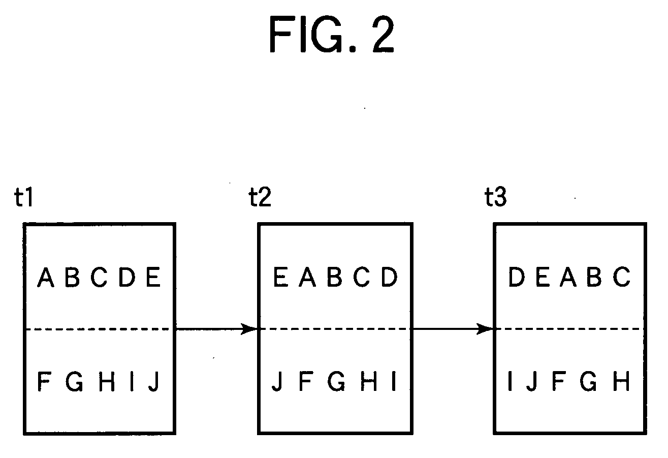
[0042]FIG. 3 shows the structure of a display panel driver in a second embodiment of the invention. This display panel driver displays a small screen saving image X that travels freely in both the horizontal and vertical directions across the entire screen area of the display panel 1, even though the screen is divided into two halves. The driver has a master chip 20m for driving the upper half A1, and a slave chip 20s for driving the lower half A2. The master chip 20m and the slave chip 20s are connected to the CPU 3 and the main memory 4 via the system bus 2 as in the first embodiment. The master chip 20m and the slave chip 20s are identical display driver LSI chips, either one of which can operate as master or slave as specified by the setting signal SET. In the following description of the structure of the master and slave chips, both chips will also be referred to as a driver chip 20m / s.

[0043] The driver chip 20m / s employs a virtual spatial coordinate system that covers both th...


PUM


Abstract

A display panel driver has two driver circuits that drive separate halves of a display panel. Each driver circuit occupies a separate integrated circuit chip. The driver has a screen saving mode in which each driver circuit displays an independent screen saving image that moves in synchronization with a timing signal. The timing signal is generated in one driver circuit and transmitted by a chip-to-chip interface to the other driver circuit. The two screen saving images are thereby coordinated to create what appears to be a single screen saving display.

Description

BACKGROUND OF THE INVENTION [0001] 1. Field of the Invention [0002] The present invention relates to a display panel driver having two large-scale integrated circuits that drive separate halves of a display panel, more particularly to a screen saving function of the display panel driver. [0003] 2. Description of the Related Art [0004] Although the flat panel displays used in devices such as mobile telephones have conventionally been liquid crystal displays (LCDs), the technology is now shifting to organic electroluminescence (EL) displays, also known as organic light-emitting diode (OLED) displays. Organic EL displays have the advantages of high visibility and good color rendition, and can be made in large sizes. While a small organic EL display can be driven by a large-scale integrated (LSI) circuit disposed on a single semiconductor chip, for larger organic EL displays a dual scan system is used in which the display screen is divided vertically or horizontally into two halves, eac...

Claims


Application Information

Patent Timeline
Patent Type & Authority Applications(United States)
IPC IPC(8): G09G5/00H05B44/00
CPCG09G3/20G09G3/3208G09G2330/022G09G2310/0221G09G2310/0205
Inventor KONDO, AKIRAKIMURA, NAOYATAKAYANAGI, HARUYOHARA, TETSUROSHIMIZU, TAKAYUKIICHKURA, HIROYOSHI
Owner LAPIS SEMICON CO LTD
Why Eureka
Try Eureka