[0006] The touch panel shown in FIG. 20 determines a region (a blackened circle), where the photoreceptive devices to be a photosensor does not receive light, by use of coordinates, and then detects a position where the finger touches. Therefore, it is required to dispose a
light source and a photosensor in a manner that on the display unit, the
light emission from the
light source is uniform and also there is no region where the
light emission does not reach. If a precision to recognize a position on which a finger touches is attempted to be increased, it is generally required to dispose many light sources and photosensors in the circumference of the display area 302. Hence, the requirement has been a factor to hinder the
miniaturization of a touch panel. Furthermore, there has been a problem such as variations in sensing sensitivity in a region where it is difficult for light to reach (for example, a point Z which is the farthest from a light source) and in the vicinity of the center.
[0006] The touch panel shown in FIG. 20 determines a region (a blackened circle), where the photoreceptive devices to be a photosensor does not receive light, by use of coordinates, and then detects a position where the finger touches. Therefore, it is required to dispose a light source and a photosensor in a manner that on the display unit, the
light emission from the light source is uniform and also there is no region where the light emission does not reach. If a precision to recognize a position on which a finger touches is attempted to be increased, it is generally required to dispose many light sources and photosensors in the circumference of the display area 302. Hence, the requirement has been a factor to hinder the
miniaturization of a touch panel. Furthermore, there has been a problem such as variations in sensing sensitivity in a region where it is difficult for light to reach (for example, a point Z which is the farthest from a light source) and in the vicinity of the center.
[0244] Third, since the display pixel and the photosensor are close to each other, it is possible to sense uniformly. The sensitivity, such as reducing variations in sensing and eliminating a region where it is difficult for light to reach, is improved.
[0245] Fourth, if one photosensor is provided for the plurality of display pixels, a region for display is enlarged.
[0246] Fifth, since it is possible to be fabricated on the same substrate in the same process, it is possible to contribute to a significant reduction in the number of parts, and reductions in manufacturing cost and the number of manufacturing processes.
[0004] Among current display devices, a
flat panel display is widespread due to market demands of reduction in size, weight and thickness. A photosensor is incorporated in many of display devices of this kind, such as, for example, an optical touch panel in which input coordinates are detected by blocking light and a device in which external light is detected to thereby control the brightness of a display screen.
[0249] Seventh, since the photosensor is constituted of a photoreceptor circuit whose sensitivity of receiving light is adjustable, it is possible to make the sensitivity of receiving light (detection) of the display unit uniform. A
photocurrent is a
dark current of when a TFT is off, and is easy that variations in detection characteristics are generated. However, since the sensitivity of receiving light is adjustable according to the embodiments of the present invention, the sensitivity of receiving light between devices can be made uniform, thus making it possible to provide a touch panel in which the characteristics are stable.
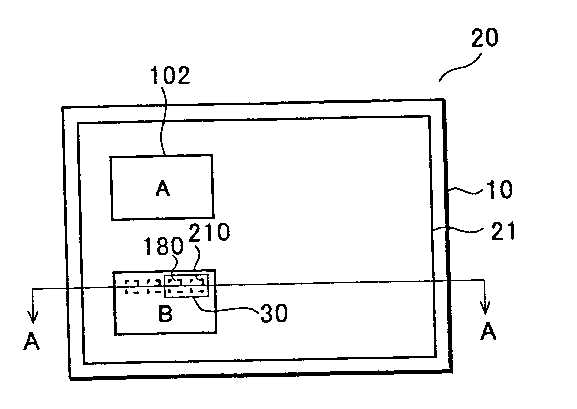
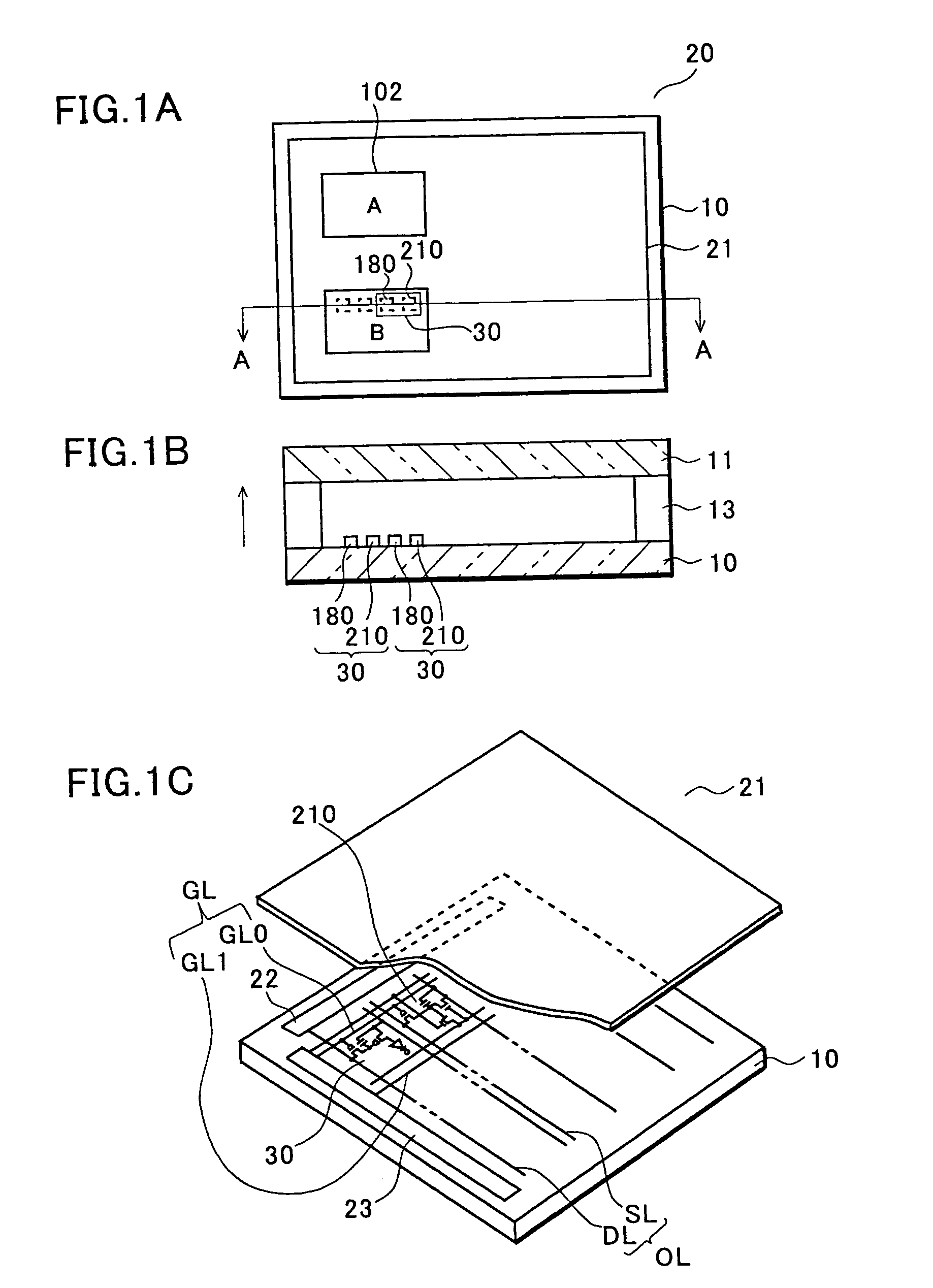
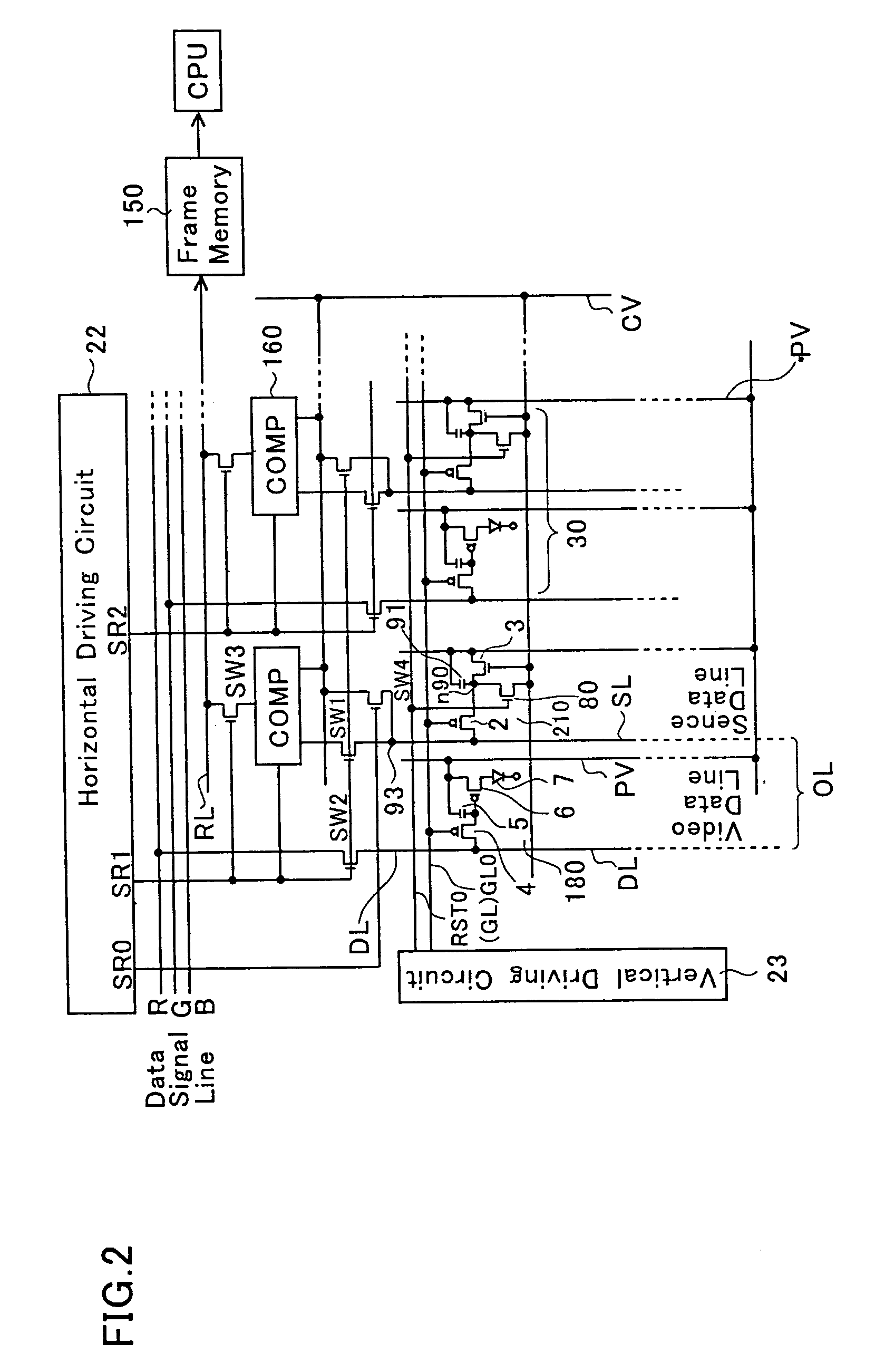
[0011] The present invention further provides a touch panel that includes, a substrate, a plurality of data output lines disposed on the substrate, a plurality of gate lines disposed on the substrate so as to intersect the data output lines, a display area comprising a plurality of display pixels disposed on the substrate, each of the display pixels comprising a light emitting circuit and being disposed adjacent a corresponding intersection of the data output lines and the gate lines, and a plurality of photosensor circuits disposed in the display area, wherein the photosensor circuits are configured to be scanned so as to identify positions of the display area in which corresponding photosensor circuits do not detect external light incident on the display area.

