
Eureka
For R&D, Eureka makes reading and utilizing patents & technical documents easy.
Eureka AIR
Designed for self-driven R&D workflows. Generate viable solutions, solve complex R&D challenges, empower your innovation with AI.

Eureka Materials
Designed for material experts only. Revolutionize your material R&D, from search, analyze, to developing new materials.

TechResearch
Generate reliable direction feasibility study reports for your R&D in just a few steps.

TechSeek
Discover and master advanced knowledge NOW. Basics, ideas, possibilities, all at once.

TechMind
As an expert in R&D Theories, TechMind can generates customized viable solutions instantly.

TechRisk
Analyze your overall solution with one click, know your potential R&D risks in advance.

TechMonitor
Get weekly tech updates, stay abreast of the latest tech innovations and key insights.
Electron emission display (EED) and method of driving the same
- Summary
- Abstract
- Description
- Claims
- Application Information
AI Technical Summary
Benefits of technology
Problems solved by technology
Method used
Image

Examples
Embodiment Construction
[0045] Hereinafter, exemplary embodiments of the present invention will be described in detail with reference to the attached drawings.
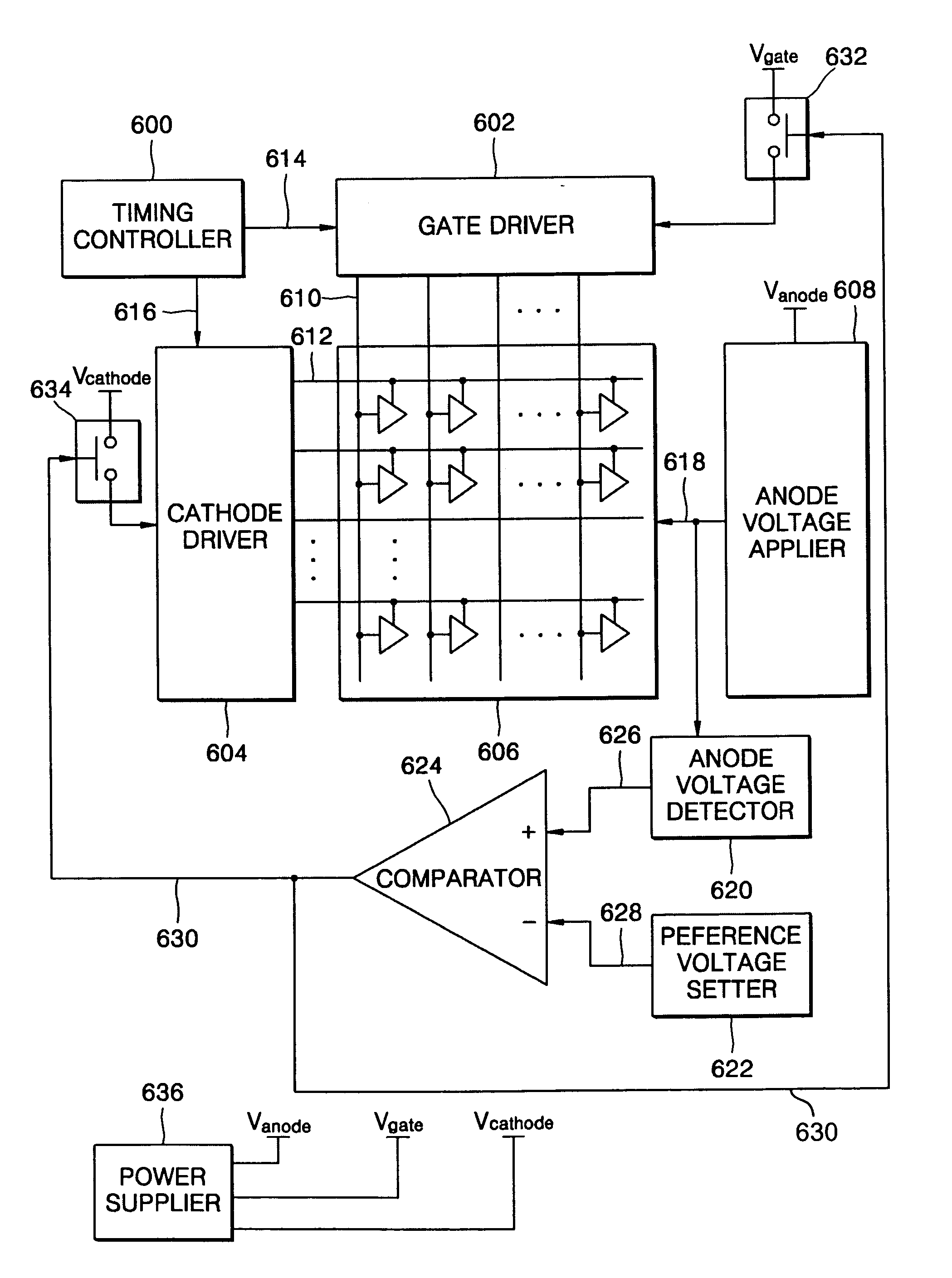
[0046] The present invention is directed to an electron emission display including a scan electrode that extends in one direction of a lattice panel, a data electrode that extends across the scan electrode, and an anode, and a method of driving the same.
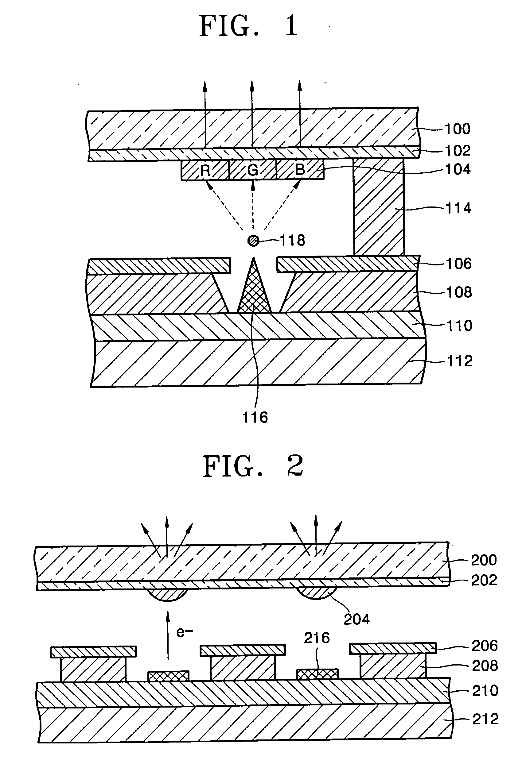
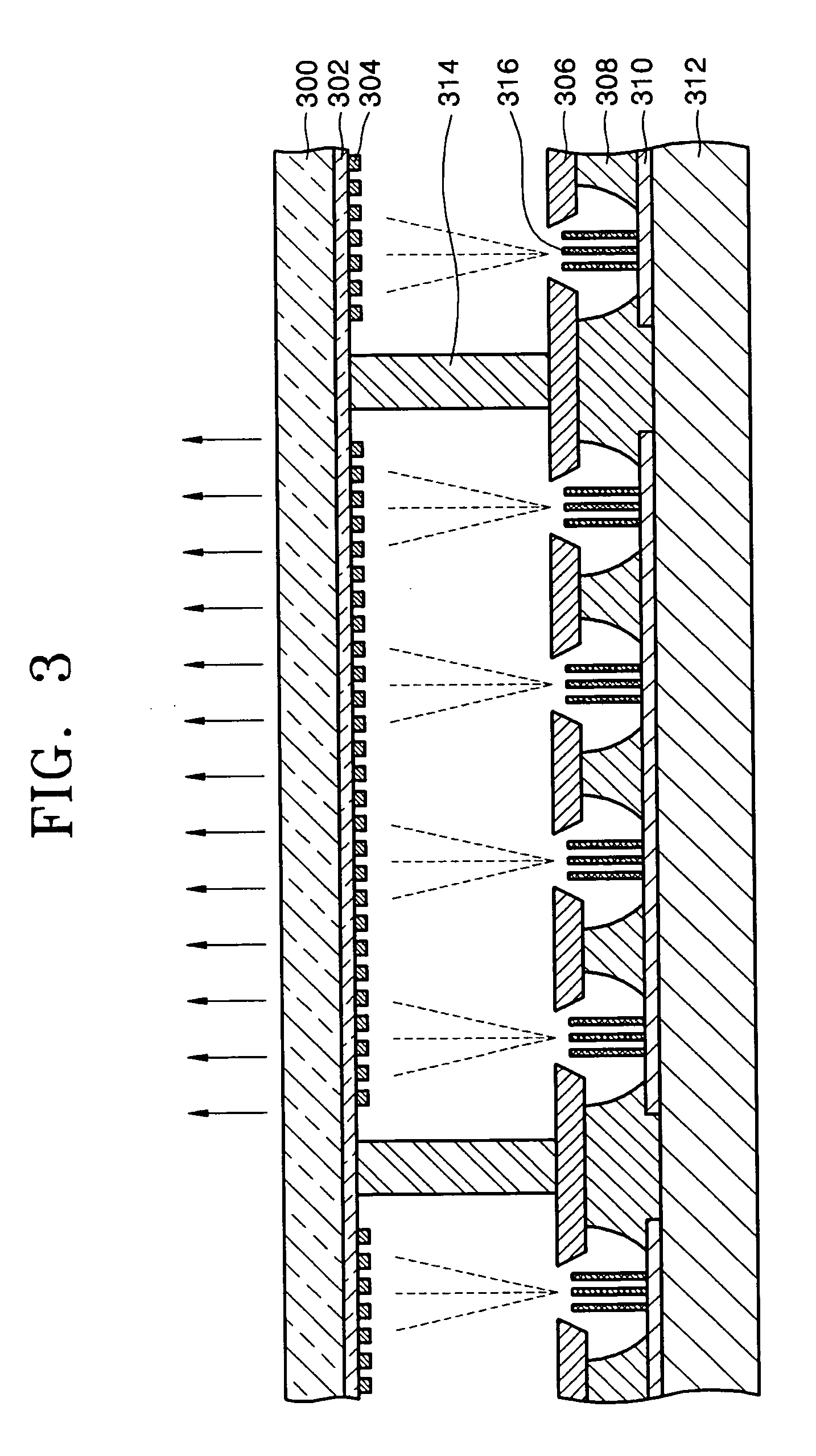
[0047] A field emission display (FED) as an example of the electron emission display will now be described.
[0048] The FED can be categorized into one having a top gate structure or one having an under gate structure based on the position of a gate electrode. The top gate structure comprises a cathode, a gate electrode, and an anode, which are sequentially disposed on a glass substrate. On the other hand, the under gate structure comprises a gate electrode, a cathode and an anode, which are sequentially disposed on a glass substrate.
[0049] The present invention can be applied to both the top gate t...
PUM
 Abstract
Description
Claims
Application Information
 - R&D Engineer
- R&D Manager
- IP Professional
- Industry Leading Data Capabilities
- Powerful AI technology
- Patent DNA Extraction
Browse by: Latest US Patents, China's latest patents, Technical Efficacy Thesaurus, Application Domain, Technology Topic, Popular Technical Reports.
© 2024 PatSnap. All rights reserved.Legal|Privacy policy|Modern Slavery Act Transparency Statement|Sitemap|About US| Contact US: help@patsnap.com