
Gate line driving circuit

Inactive Publication Date: 2006-02-23
TOSHIBA MATSUSHITA DISPLAY TECH
View PDF7 Cites 39 Cited by
  • Summary
  • Abstract
  • Description
  • Claims
  • Application Information

AI Technical Summary

Benefits of technology

[0013] The object of the present invention is to provide a gate line driving circuit that is capable of solving a problem of incomplete transition of a pixel voltage due to the time constant of a gate line in black insertion driving for maintaining the bend alignment of liquid crystal molecules.
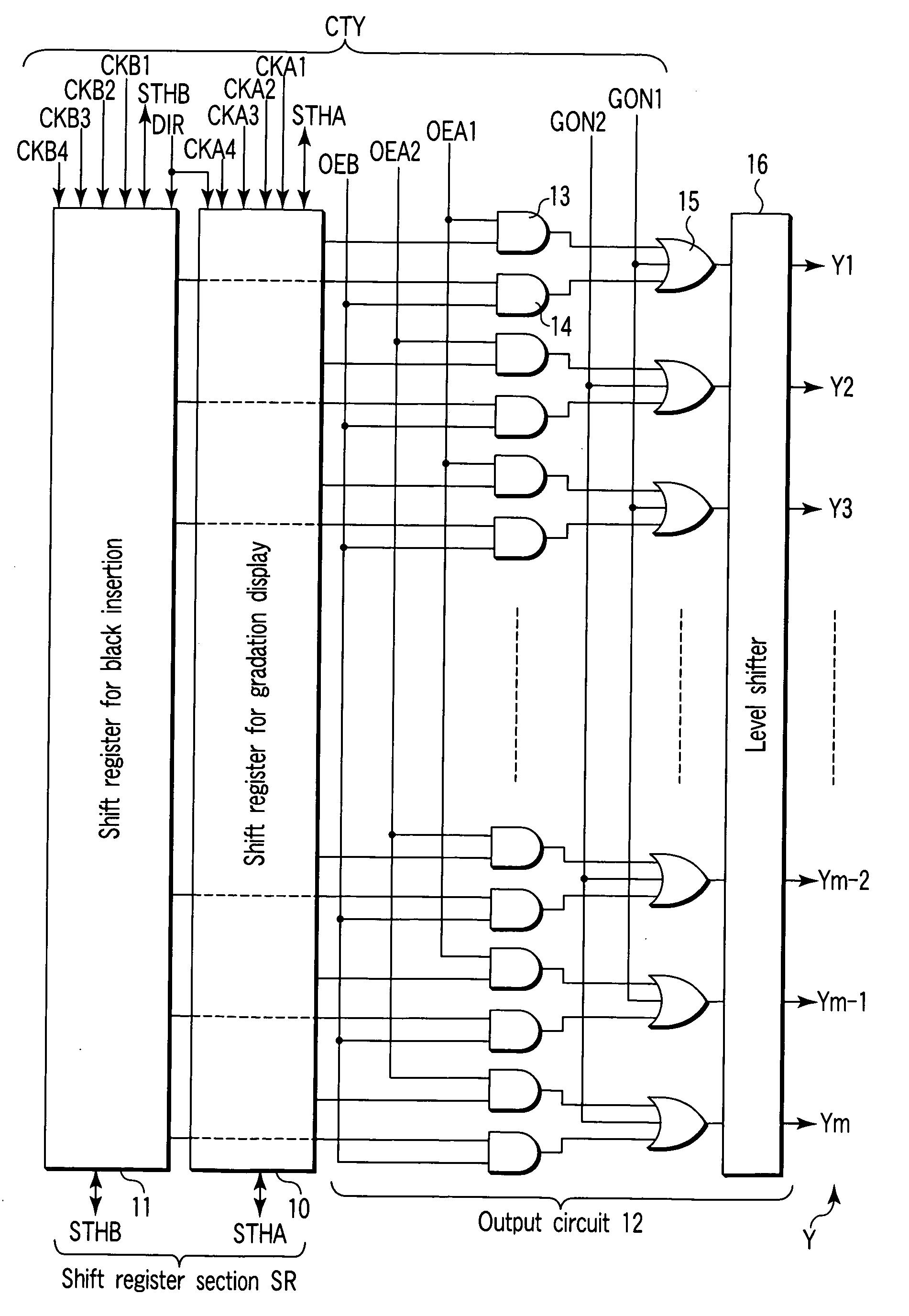
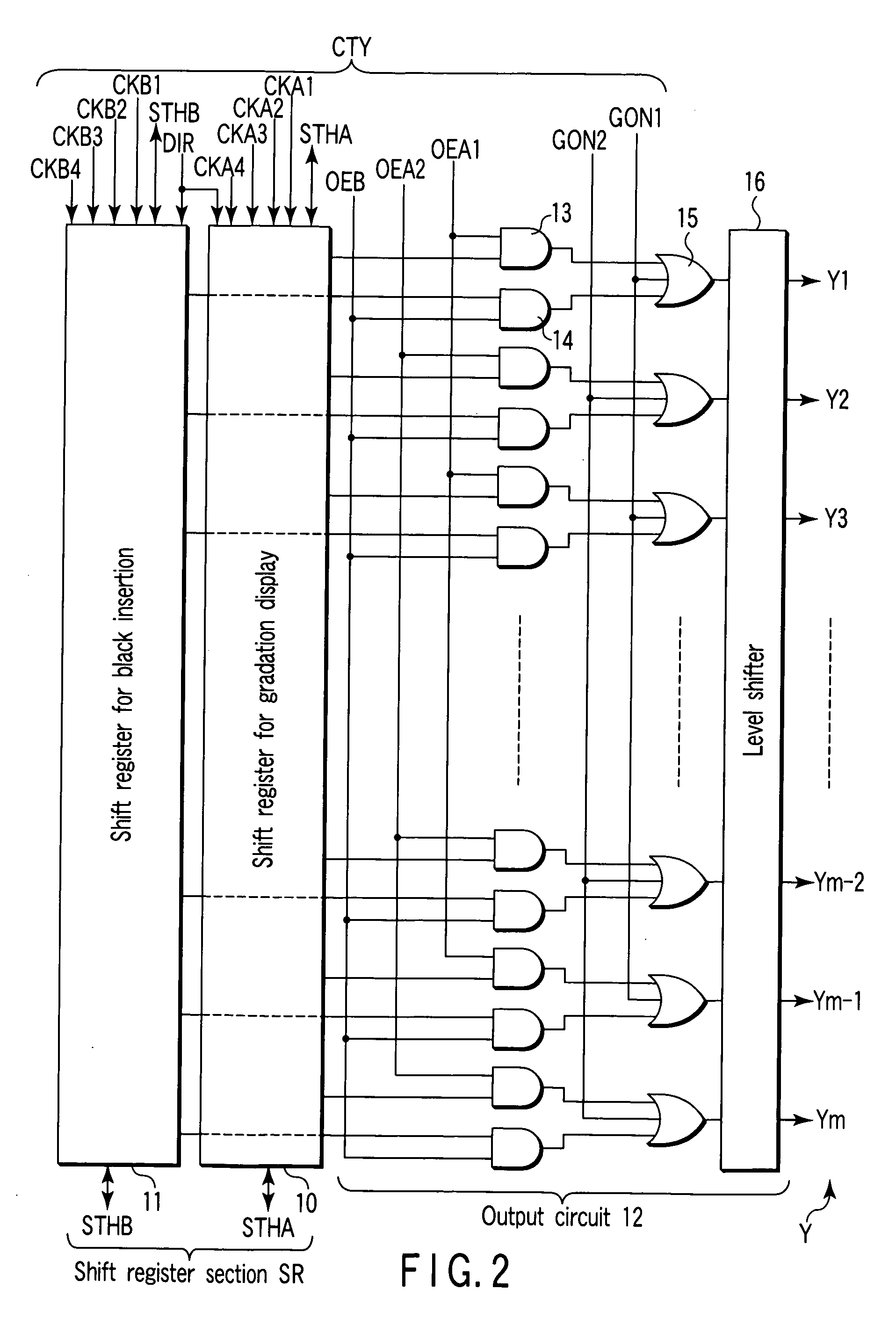
[0015] With the gate line driving circuit, an overlap is obtained between the output period of the driving signal to each gate line and the output period of the driving signal to the gate line that is driven in precedence to the selected gate line, and the first preliminary driving period and the second preliminary driving period are independently controlled. Specifically, even in the case where each gate line has a large time constant depending on the wiring resistance or parasitic capacitance and a transition in potential corresponding to the driving signal requires a significant length of time, the transition in the potential of the gate line selected for gradation display begins during a driving operation of a gate line that is driven in precedence, and the transition in the potential of the gate line selected for non-gradation display begins during a driving operation of a gate line that is driven in precedence. Thus, each of the potentials of the gate lines selected for gradation display and for non-gradation display is set to a desired value within the first or second preliminary driving period, thereby solving deficiency in transition of a pixel voltage to be applied to the associated pixel.

Problems solved by technology

In particular, in a large-sized panel of, e.g. 32 inches, the time constant, which depends on the wiring resistance and parasitic capacitance of the gate line, increases, and the rising of the gate line potential corresponding to the driving signal, which is output from the gate driver to the gate line, becomes dull.
Thus, there is a tendency that the pixel voltage of the liquid crystal pixel cannot transit to a level equal to the source line potential during this driving period.

Method used


Image

  • Gate line driving circuit
  • Gate line driving circuit
  • Gate line driving circuit

Examples


Embodiment Construction

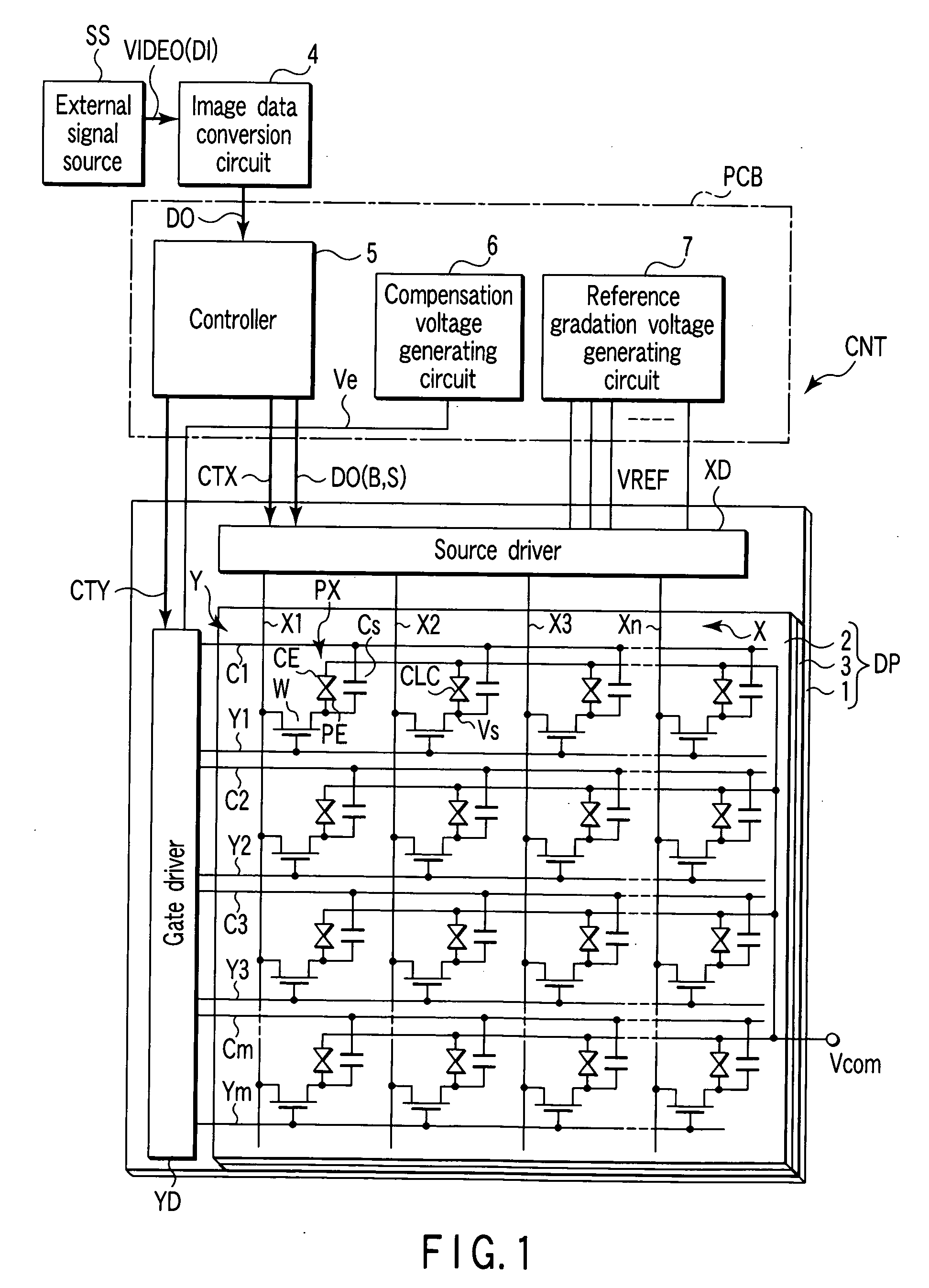
[0022] A liquid crystal display device according to an embodiment of the present invention will now be described with reference to the accompanying drawings. FIG. 1 schematically shows the circuit configuration of the liquid crystal display device. The liquid crystal display device comprises a liquid crystal display panel DP and a display panel control circuit CNT that is connected to the display panel DP. The liquid crystal display panel DP has a large size of, e.g. 32 inches in diagonal, and is configured such that a liquid crystal layer 3 is held between an array substrate 1 and a counter-substrate 2, which are a pair of electrode substrates. The liquid crystal layer 3 contains a liquid crystal material whose liquid crystal molecules are transferred in advance from a splay alignment to a bend alignment usable for a normally-white display, and are prevented from being inverse-transferred from the bend alignment to the splay alignment by a voltage for black insertion (non-gradation...


PUM


Abstract

A gate line driving circuit includes a shift register section that selects gate lines for gradation display and for black insertion, and an output circuit that outputs a driving signal to the gate line which is selected by the shift register section. In particular, the output circuit is configured to obtain an overlap between an output period of a driving signal to each selected gate line and an output period of a driving signal to a gate line that is driven in precedence to the selected gate line, and independently control a first preliminary driving period corresponding to the overlap for gradation display and a second preliminary driving period corresponding to the overlap for black insertion.

Description

CROSS-REFERENCE TO RELATED APPLICATIONS [0001] This application is based upon and claims the benefit of priority from prior Japanese Patent Application No. 2004-240799, filed Aug. 20, 2004, the entire contents of which are incorporated herein by reference. BACKGROUND OF THE INVENTION [0002] 1. Field of the Invention [0003] The present invention relates to a gate line driving circuit that is applied to an OCB (Optically Compensated Birefringence) mode liquid crystal display panel. [0004] 2. Description of the Related Art [0005] Flat-panel display devices, which are typified by liquid crystal display devices, have widely been used as display devices for computers, car navigation systems, TV receivers, etc. [0006] The liquid crystal display device generally includes a liquid crystal display panel including a matrix array of liquid crystal pixels, and a display panel control circuit that controls the display panel. The liquid crystal display panel is configured such that a liquid crysta...

Claims


Application Information

Patent Timeline
IPC IPC(8): G09G3/36
CPCG09G3/3677G09G2310/02G09G2320/0223G09G2310/06G09G2310/061G09G2310/0245
Inventor NAKAMURA, TETSUYAKAWAGUCHI, SEIJITAKEOKA, MASAHIKO
Owner TOSHIBA MATSUSHITA DISPLAY TECH
Learn More