Page buffer for a programmable memory device

a programmable memory and buffer technology, applied in the field of solid-state memories, can solve the problems of affecting the known page buffer, and requiring more complex operations

Active Publication Date: 2006-02-23
STMICROELECTRONICS SRL +1
View PDF8 Cites 61 Cited by
  • Summary
  • Abstract
  • Description
  • Claims
  • Application Information

AI Technical Summary

Benefits of technology

[0016] In view of these drawbacks, it is an object of the present invention to provide an impro

Problems solved by technology

However, more complex operations may be desirable and required, and in these cases the structure of the page buffer may need to be upgraded.
There has been identified some problems affecting the known page buffers.
This may cause the latch to be incapable of driving the bitline in a way that is sufficient to cause the programming into the desired state of the selected memory cell (the latch is not capable of bringing the bitline from the initial, program inhibition voltage to a voltage adapted to cause programming of the selected memory cell) and, in the worst cases, the latch may even be caused to

Method used


Image

  • Page buffer for a programmable memory device
  • Page buffer for a programmable memory device
  • Page buffer for a programmable memory device

Examples


Embodiment Construction

[0023] Preferred embodiments of the present invention will be described in detail hereinbelow with reference to the attached drawings.

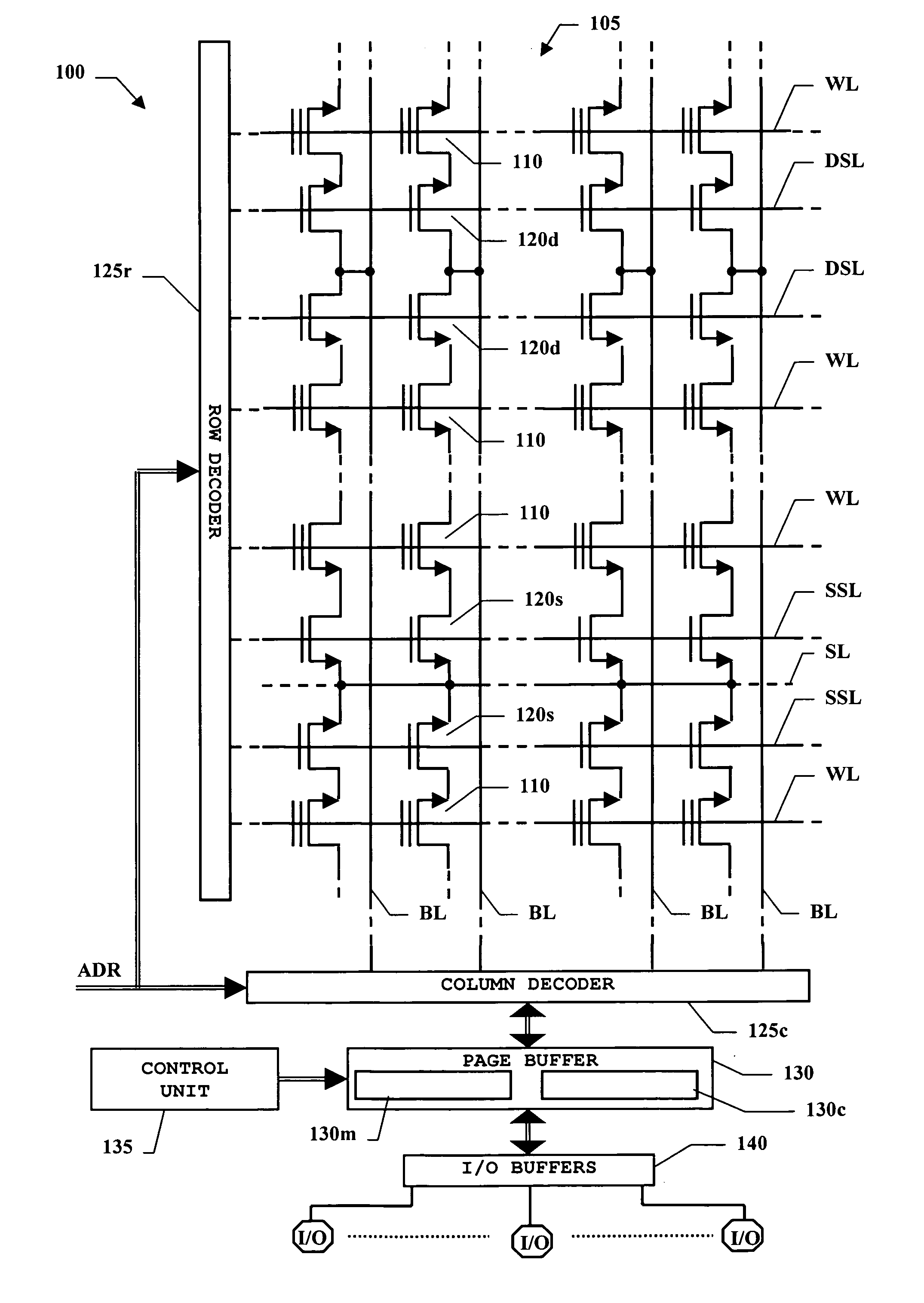
[0024]FIG. 1 illustrates a non-volatile semiconductor memory 100 according to a preferred embodiment of the present invention. The memory 100 is an electrically-programmable, non-volatile semiconductor memory, for example a flash memory.

[0025] The flash memory 100 is integrated in a chip of semiconductor material, and includes a matrix 105 of memory cells 110 arranged in a plurality of rows and a plurality of columns.

[0026] In this embodiment, each memory cell 110 consists of an N-channel MOS transistor having a charge-storage element, such as a conductive floating gate that is adapted to be charged by injected electrons. Without going into excessive detail, in an erased condition (associated by convention with a stored logic value of “1”), the memory cell 110 has a low threshold voltage value. The memory cell 110 is programmed by injecting electri...


PUM


Abstract

A page buffer is provided for an electrically programmable memory that includes multiple memory cells forming multiple memory pages. The page buffer includes a register for at least temporarily storing data read from or to be written to the memory cells of a selected memory page. The register includes multiple latches and multiple buffer elements. Each of the latches is coupled to at least one signal line for transferring the data bit that is stored in the latch. Each of the buffer elements decouples an output of a corresponding one of the latches from the signal line, with the buffer element driving the signal line according to the data bit stored in the corresponding latch. Also provided is a method of transferring data from a register to signal lines in an electrically programmable memory.

Description

CROSS-REFERENCE TO RELATED APPLICATIONS [0001] This application is based upon and claims priority from prior European Patent Application No. 04 102 232.8, filed May 20, 2004, the entire disclosure of which is herein incorporated by reference. FIELD OF THE INVENTION [0002] The present invention generally relates to the field of solid-state memories, particularly to semiconductor memories, and even more particularly to the field of non-volatile memories that are electrically programmable. BACKGROUND OF THE INVENTION [0003] Non-volatile memories are commonly used in several applications in which the data stored in the memory device needs to be preserved even in the absence of a power supply. Within the class of non-volatile memories, electrically programmable (and erasable) memories, such as flash memories, have become very popular in applications in which the data to be stored is not immutable (e.g., in the case of a consolidated code for a microprocessor), but it is instead necessary...

Claims


Application Information

Patent Timeline
IPC IPC(8): G11C16/04G11C16/10G11C16/26
CPCG11C16/26
Inventor KHOURI, OSAMAZANARDI, STEFANOMARTINOZZI, GIULIO
Owner STMICROELECTRONICS SRL
Why Eureka
Try Eureka