Unlock instant, AI-driven research and patent intelligence for your innovation.

Method and apparatus for inspecting substrate pattern

Inactive Publication Date: 2006-02-23
SAMSUNG ELECTRONICS CO LTD
View PDF5 Cites 16 Cited by
  • Summary
  • Abstract
  • Description
  • Claims
  • Application Information

AI Technical Summary

Benefits of technology

[0017] Embodiments of the present invention provide a method of inspecting an inspection pattern on a substrate capable of inspecting pattern defects in the inspection pattern without the requirement for accurately measuring the physical properties of the inspection pattern. Embodiments of the invention also provide an apparatus for performing the this method.

Problems solved by technology

These even smaller dimensions are increasingly intolerant to design and manufacturing errors.
Yet, such ever smaller defects are harder and harder to identify during quality assurance processes.
For example, common processing defects include voids formed in an insulation interlayer and a bridge defect formed on the contact plug of a stacked capacitor structure.
As the overall dimensions of these individual components have shrunk over time, the associated processing defects have become ever more small and difficult to locate.
Most processing defects are caused by a pattern defect.
Unfortunately, the SEM measurement requires a vacuum state and a lengthy examination period in order to provide satisfactory inspection results.
The slow rate of inspection provided by SEM measurements is particularly disadvantageous in the context of modern manufacturing facilities which require highly efficient processes in order to ensure commercially viable productivity.
However, the conventional optical measurement technique has a great difficulty analyzing the large number of reflected optical signals generated by more complicated inspection patterns.
Indeed, such analysis typically requires the use of a costly computer server to process a large number of complex, reflected optical signals.
Yet, an accurate measurement on the physical properties of an inspection pattern is not necessarily required for the detection of pattern defects, and further reliance on the examination of physical properties will only become ever more fruitless as pattern designs are defined in smaller and smaller dimensions.
Unfortunately, this disclosure has a problem in that the optimal reflection light and the optimal pattern have no unique correspondence with each other, since an accurate statistical analysis correlating the reflection light and physical properties of the inspection pattern are not usually known.
Yet, unfortunately, this disclosure has limited utility to only those inspection patterns having clear periodic features repeated across the substrate since the surface ratio of the inspection pattern is obtained from the ratio of the inspection pulse with respect to the output pulse.
Accordingly, the inspection method proposed in this Japanese laid-open patent document cannot be applied to inspection patterns lacking such periodic features.
These disclosures are but two examples of the many inadequate attempts previously made to develop an improved method of inspecting for defects in an inspection pattern without the requirement of accurately measuring the physical properties of the inspection pattern.

Method used


Image

  • Method and apparatus for inspecting substrate pattern
  • Method and apparatus for inspecting substrate pattern
  • Method and apparatus for inspecting substrate pattern

Examples


Embodiment Construction

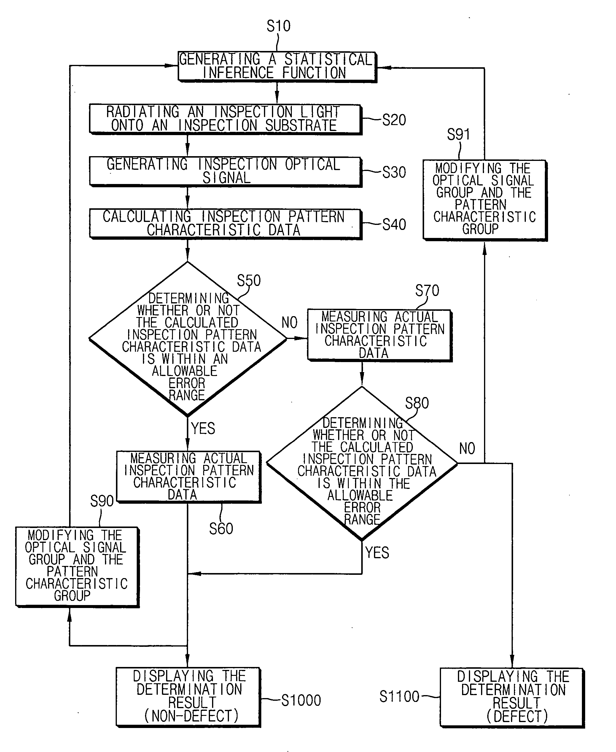
[0044] As will be set forth in some additional detail below, the inspection pattern characteristic data provided by the invention is calculated from a statistical inference function and related optical inspection signal data. Based on this data, a determination is made as to whether or not a related inspection pattern has been formed by a unit process of interest with an allowable error tolerance range. By use of an embodiment implemented according to the dictates of the invention, the cost and time associated with the inspection process are remarkably reduced.

[0045] In additional embodiments of the invention, the optical reference signal data and the inspection pattern characteristic data actually measured during the inspection process are accumulated in order to established optical signal group(s) and pattern characteristic group(s), so that confidence in the inference function is improved over time. As a result, although an inspection process adapted to examine the inspection pa...


PUM


Abstract

A method of inspecting an inspection pattern using a statistical inference function is disclosed. The inference function is generated in relation to optical reference signal data and reference pattern characteristic data for a plurality of reference patterns formed by a unit process of interest on reference substrates.

Description

BACKGROUND OF THE INVENTION [0001] 1. Field of the Invention [0002] The present invention relates to an apparatus adapted to inspect a pattern on a substrate and a related method. More particularly, the invention relates to a method and apparatus adapted to inspect a pattern characteristic using a statistical inference function using a light signal corresponding to the pattern characteristic. [0003] This application claims the benefit of Korean Patent Application No. 2004-66203 filed on Aug. 23, 2004, the subject matter of which is hereby incorporated by reference in its entirety. [0004] 2. Description of the Related Art [0005] As semiconductor devices have become more highly integrated and operating speeds have increased, design rules have changed. In general, a contact area and other critical dimensions defining the layout of contemporary semiconductor devices have gradually been reduced. These even smaller dimensions are increasingly intolerant to design and manufacturing errors....

Claims


Application Information

Patent Timeline
IPC IPC(8): G06K9/00
CPCG01N21/21G01N21/33G01N2021/95615G01N21/95607G01N21/9501H01L22/00
Inventor KIM, KYE-WEONJUN, CHUNG-SAMCHUNG, KI-SUKCHON, SANG-MUNKIM, SEONG-JINLEE, BYUNG-SUGYANG, YU-SIN
Owner SAMSUNG ELECTRONICS CO LTD