Renesting interaction map into design for efficient long range calculations

a technology of interaction map and design data, applied in the field of optical lithography, can solve the problems of reducing circuit performance, reducing the efficiency of circuits, so as to avoid flattening of the desired design data hierarchy, efficient, easily and cost effective, and efficiently and cost effective the effect of rebuilding the design data hierarchy

Active Publication Date: 2006-02-23
GLOBALFOUNDRIES US INC
View PDF21 Cites 9 Cited by
  • Summary
  • Abstract
  • Description
  • Claims
  • Application Information

AI Technical Summary

Benefits of technology

[0017] It is another object of the present invention to provide a model-based approach that efficiently, easily and cost effectively maintains a desired design data hierarchy regardless of ROI size.
[0018] Another object of the present invention is to provide a model-based approach that efficiently, easily and cost effectively rebuilds a design data hierarchy when a desired design data hierarchy is destroyed.
[0019] Yet another object of the present invention is to provide a model-based approach that avoids flattening of the desired design data hierarchy such that flare calculations can be applied to the model-based simulation.
[0020] A further object of the invention is to provide a model-based approach for enforcing a design data hierarchy that saves both processing time and memory.
[0022] Yet another object of the invention is to provide a model-based approach for enforcing a design data hierarchy that provides stability in model-based optical lithography engines and calculations.

Problems solved by technology

Since present lithography tools employ partially coherent illumination, such modeling is computationally intensive for all but elementary patterns.
However, optical proximity correction simulation kernels associated with lithographic processes for semiconductor chip manufacturing currently do not take into account the higher order aberrations, whose results may be realized in long-range effects, although not as prominent in the close-range of 1 to 2 micrometers.
Where flare effects are constant, a dose shift compensates for its effects completely; however, wherein it is not constant, any unacceptable variation in flare effects can diminish the circuit performance, and ultimately cause catastrophic failure.
However, representing each such shape separately poses a great challenge to the computer algorithms that are used on such mask shapes.
However, when the mask design needs to consider the very long range effect such as optical or chemical flare the interaction range becomes extremely large and consequently the neighborhoods of shapes that need to be regrouped becomes very large.
However, semiconductor wafer processes often catastrophically destroy the design data hierarchy, such as those involving long-range effects, where large regions of interest (ROI) are being exposed to such semiconductor processing steps.
If unaccounted for, these long-range flare effects ultimately destroy the design data hierarchy by erosion.
Further, the larger the ROI around any given feature within the design hierarchy, the faster such feature will flatten by erosion.
For example, in the steps of computing density maps for any given level within the design hierarchy, any generated flare effects will cause a flatten or destruction of the design data hierarchy.
As a result, without special handling, semiconductor processing steps that involve long-range effects, such as flare, can make the desired design hierarchy unachievable.
Unfortunately, the prior art has been hindered by the lack of solutions for enforcing a desired design data hierarchy for long-range calculations.
Further, as it is necessary to determine and compensate for any flare effects, flattening of the desired design data hierarchy can prevent applying calculation to correct for any flare effects.

Method used


Image

  • Renesting interaction map into design for efficient long range calculations
  • Renesting interaction map into design for efficient long range calculations
  • Renesting interaction map into design for efficient long range calculations

Examples


Embodiment Construction

)

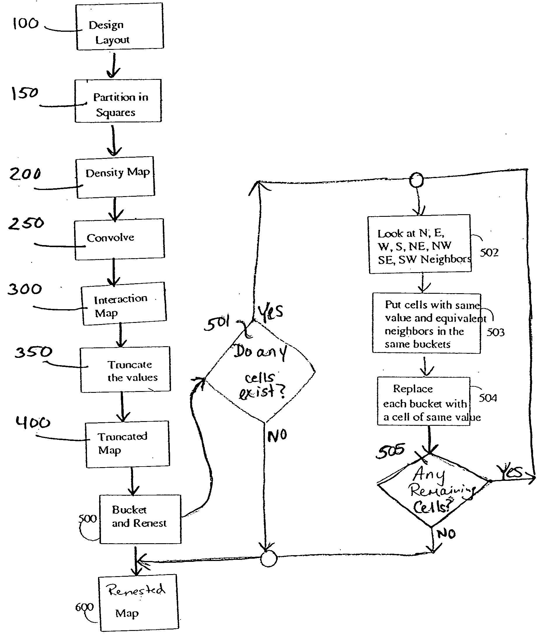
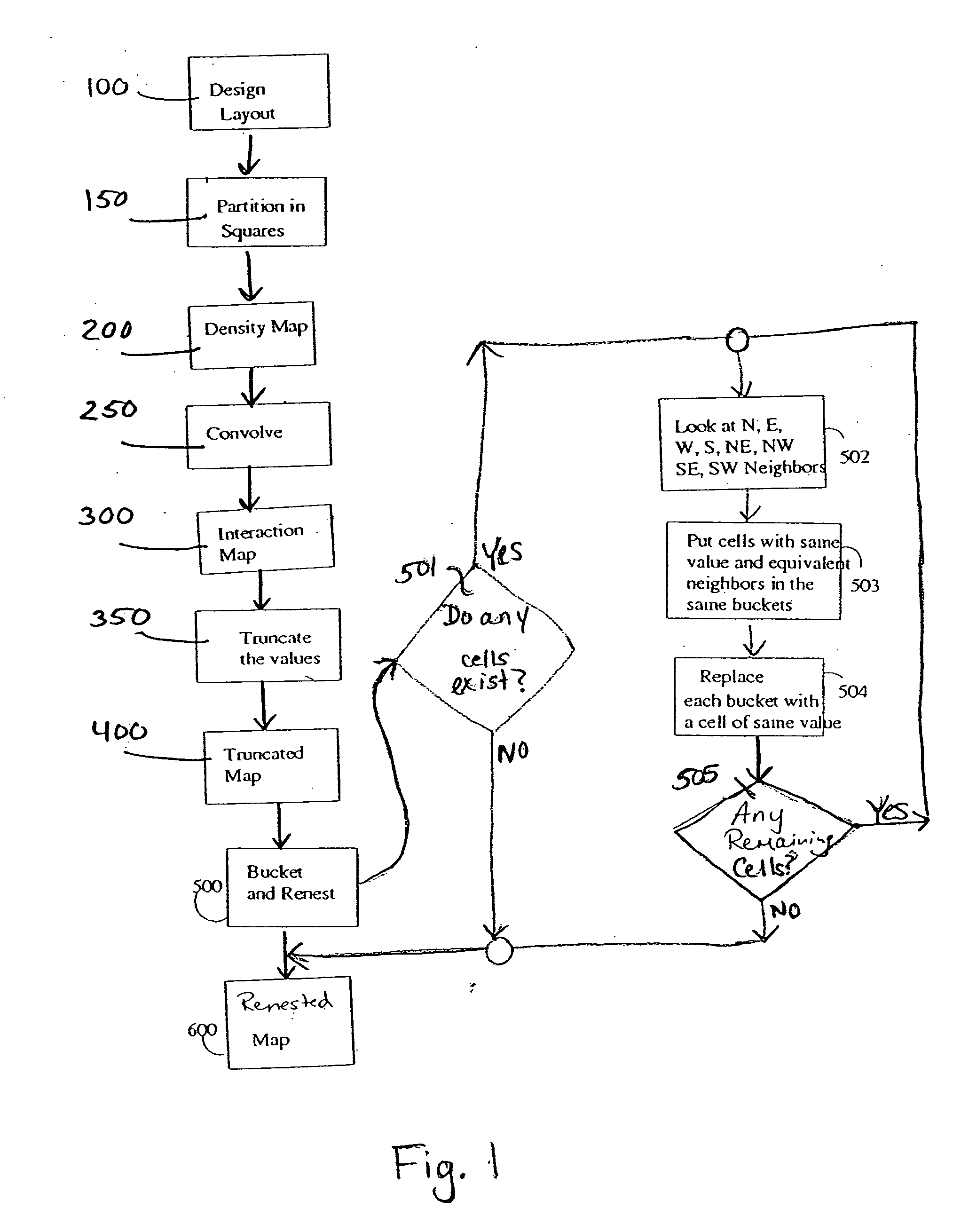
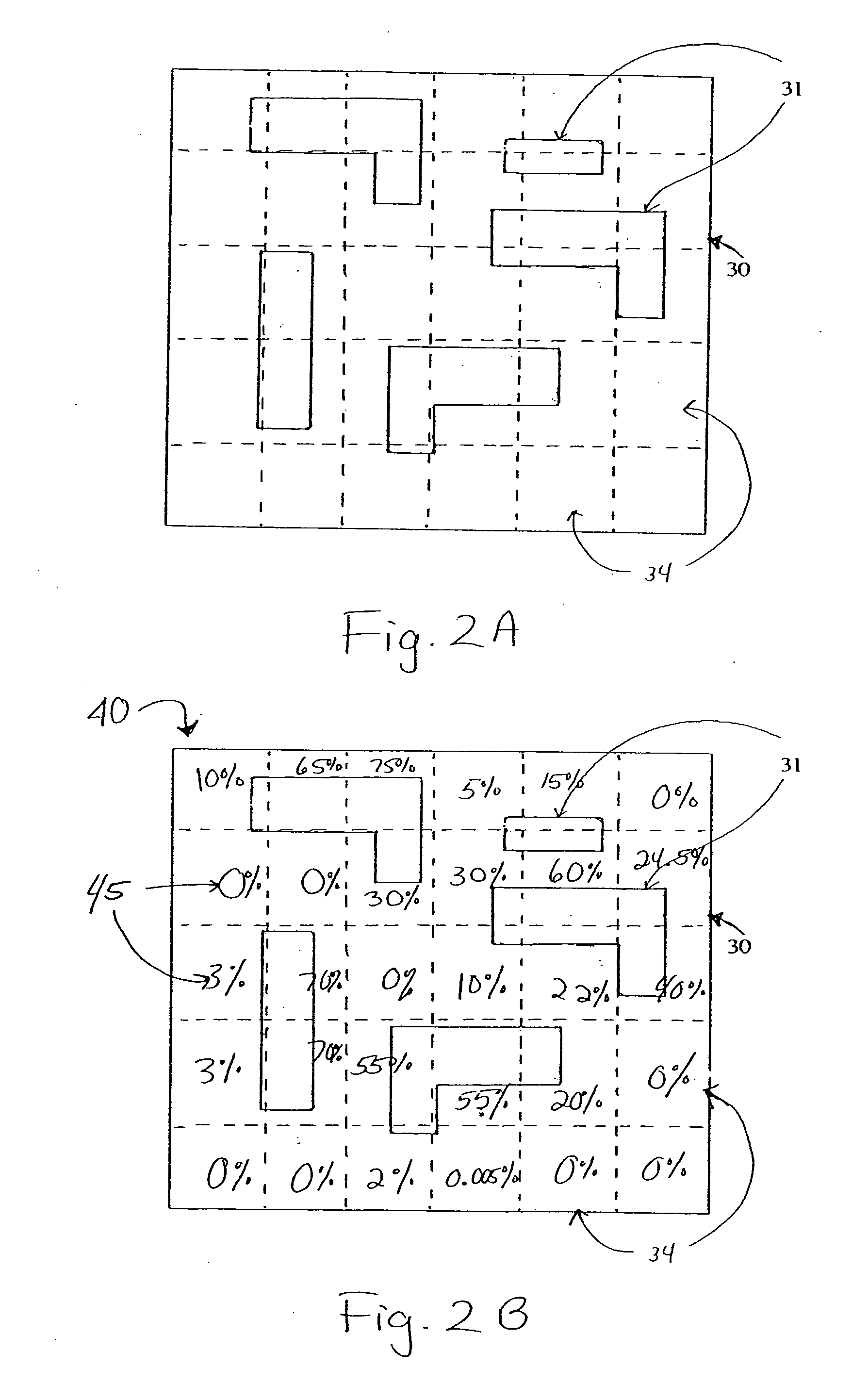
[0041] In describing the preferred embodiment of the present invention, reference will be made herein to FIGS. 1-4C of the drawings in which like numerals refer to like features of the invention.

[0042] The foregoing invention is ultimately for use in optical lithography to correct for any distortions on a photomask having desired circuit patterns, for the accurate projection thereof onto photoresist-coated wafers. In so doing, the invention provides model-based optical lithography simulations that enforce a desired design data hierarchy for long-range calculations, regardless of the size of the region of interest (ROI).

[0043] In accordance with the invention, the desired design data hierarchy is enforced by either maintaining an original, desired design data hierarchy or by rebuilding a design data hierarchy when the original, desired design data hierarchy has been either partially or completely destroyed, such as by processing conditions. However, the invention is particularly u...


PUM

PropertyMeasurementUnit
wavelengthsaaaaaaaaaa

Abstract

Methods, and program storage devices, for performing model-based optical lithography corrections by partitioning a cell array layout, having a plurality of polygons thereon, into a plurality of cells covering the layout. This layout is representative of a desired design data hierarchy. A density map is then generated corresponding to interactions between the polygons and plurality of cells, and then the densities within each cell are convolved. An interaction map is formed using the convolved densities, followed by truncating the interaction map to form a map of truncated cells. Substantially identical groupings of the truncated cells are then segregated respectively into differing ones of a plurality of buckets, whereby each of these buckets comprise a single set of identical groupings of truncated cells. A hierarchal arrangement is generated using these buckets, and the desired design data hierarchy enforced using the hierarchal arrangement to ultimately correct for optical lithography.

Description

CROSS-REFERENCE TO RELATED APPLICATIONS [0001] The present application is related to commonly assigned U.S. patent application Ser. No. 10 / 694,466, U.S. patent application Ser. No. 10 / 694,465, U.S. patent application Ser. No. 10 / 694,473, and U.S. patent application Ser. No. 10 / 694,299, filed on even date herewith, which are hereby incorporated by reference herein in their entirety.BACKGROUND OF THE INVENTION [0002] 1. Field of the Invention [0003] This invention relates generally to the field of optical lithography, and in particularly, to an approach for enforcing a design data hierarchy for long-range calculations, regardless of the size of the Region Of Interest (ROI), for use in model-based optical lithography simulations and Optical Proximity Correction (OPC). [0004] 2. Description of Related Art [0005] The optical microlithography process in semiconductor fabrication, also known as the photolithography process, consists of duplicating desired circuit patterns onto semiconducto...

Claims


Application Information

Patent Timeline
Patent Type & Authority Applications(United States)
IPC IPC(8): G06F17/50G03F1/08G03F1/14G03F7/20H01L21/027H01L21/82
CPCG03F1/144G06F17/5068G03F1/36G03F1/68G06F30/39
Inventor GALLATIN, GREGG M.GOFMAN, EMANUELLAI, KAFAILAVIN, MARK A.MUKHERJEE, MAHARAJRAMM, DOVROSENBLUTH, ALAN E.SHLAFMAN, SHLOMO
Owner GLOBALFOUNDRIES US INC
Why Eureka
Try Eureka