Bottom side stiffener probe card

a probe card and bottom side technology, applied in the field of integrated circuit testing using probe cards, can solve the problems of inconsistency, false negative, and more critical test of ics, and achieve the effect of minimizing the casting of shadows

Active Publication Date: 2006-03-02
MICRON TECH INC
View PDF15 Cites 26 Cited by
  • Summary
  • Abstract
  • Description
  • Claims
  • Application Information

AI Technical Summary

Benefits of technology

[0008] An exemplary embodiment of the invention provides a probe card for production testing of semiconductor imaging die. The probe card includes a stiffener supported on a bottom side of the probe card, nearest the imaging die being tested. The top of the stiffener is substantially flush with a top surface of the probe card. A light passage through the stiffener is provided with non-reflective surfaces. Surfaces surrounding the light passage are arranged to minimize the casting of any shadows on the imaging die being tested. The arrangement provides a low profile probe card. A light source shining through the passage in the stiffener can be placed close to the imaging die for use during active testing, providing few false negatives and more consistent results from wafer to wafer.

Problems solved by technology

As semiconductor ICs become increasingly smaller and production levels increase, testing of the ICs becomes more difficult, and more critical.
In the past, stiffeners provided on the top side of probe cards for imaging die have contributed to inconsistent lighting during testing, which has lead to inconsistencies and false-negative results.

Method used


Image

  • Bottom side stiffener probe card
  • Bottom side stiffener probe card
  • Bottom side stiffener probe card

Examples


Embodiment Construction

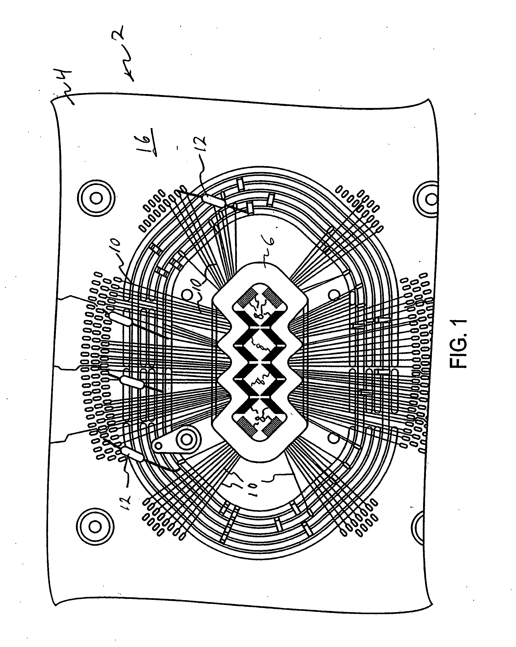
[0019] Referring to FIGS. 1-9, a probe card 2 according to an exemplary embodiment of the invention includes a printed circuit board 4 having a central opening framed by a stiffener 6. A plurality of probes 8 are supported by the stiffener 6. The probes 8 are arranged to contact peripheral pads formed on imaging die in a silicon wafer, as described further below. The probes are secured to the stiffener 6 by a layer of adhesive, such as epoxy 7. Individual probes 8 are connected by leads 10 to circuitry provided on the printed circuit board 4. Portions of the probes and their connections to leads 10 are encased in epoxy 7, as indicated for representative probes by broken lines 9. Some of the circuitry, which is not shown in detail in the Figures, includes discrete components such as capacitors 12.

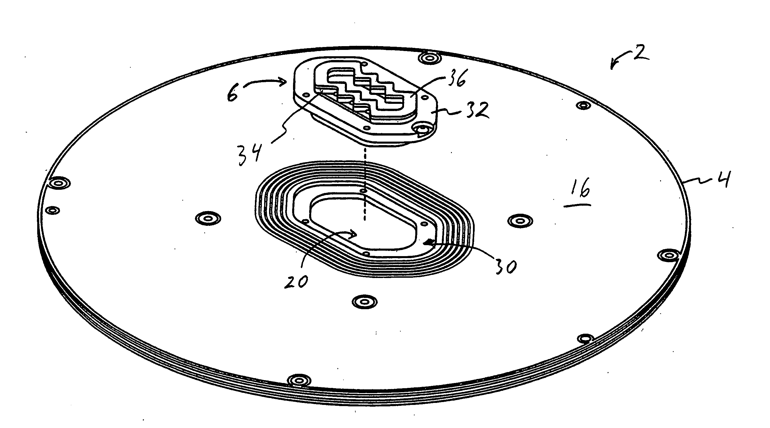
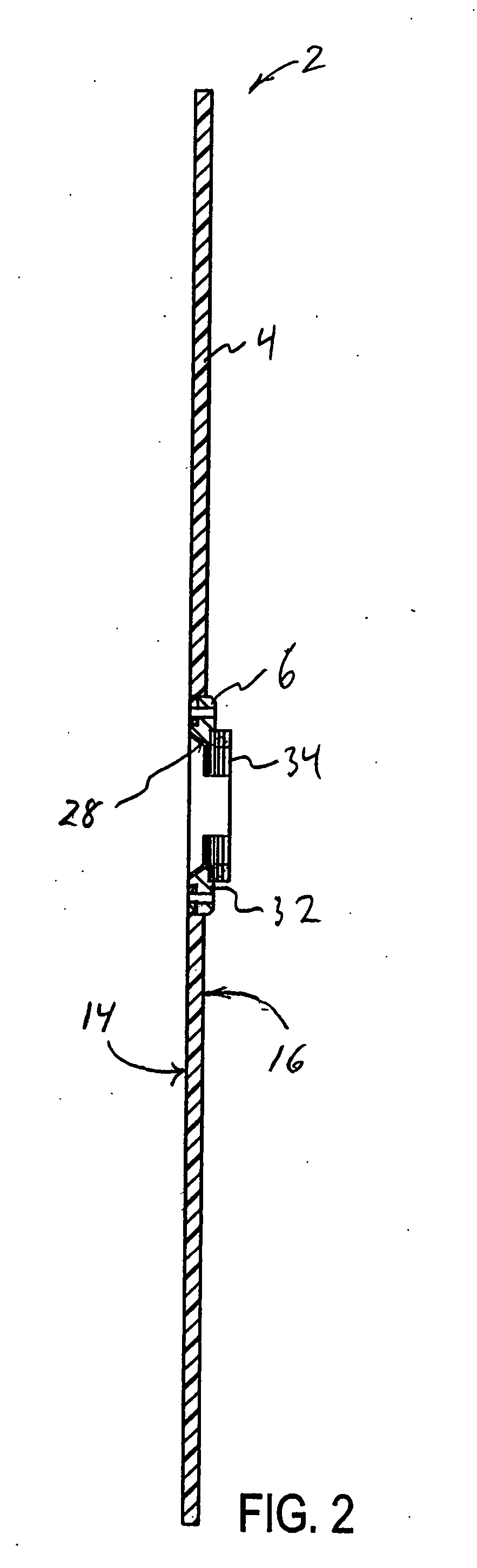
[0020] Referring to FIG. 2, the probe card 2 is shown in cross-section. The printed circuit board 4 includes a top side 14 and a bottom side 16. The stiffener 6 is disposed substantially fl...


PUM

PropertyMeasurementUnit
temperaturesaaaaaaaaaa
thicknessaaaaaaaaaa
shapeaaaaaaaaaa

Abstract

A probe card for production testing of semiconductor imaging die includes a stiffener supported on a bottom side of the probe card. The top of the stiffener is substantially flush with a top surface of the probe card. A light passage through the stiffener features non-reflective surfaces. Surfaces surrounding the light passage are arranged to avoid casting any shadows on the imaging die being tested. The arrangement provides a low profile probe card. A source of light used to illuminate the imaging die through the light passage can be placed close to the imaging device under test, providing few false negatives and more consistent results from wafer to wafer.

Description

BACKGROUND OF THE INVENTION [0001] 1. Field of the Invention [0002] The invention relates to testing of integrated circuits using probe cards, and more particularly to bottom side stiffeners for probe cards used in production testing of wafers containing imaging die. [0003] 2. Description of the Related Art [0004] Semiconductor integrated circuits (ICs) are produced extensively and are used in a vast number of products. As semiconductor ICs become increasingly smaller and production levels increase, testing of the ICs becomes more difficult, and more critical. [0005] ICs are mass-produced on round, thin sheets of semiconducting material referred to as wafers. Wafers most commonly are made of silicon. Anywhere from 50 to 200 or more identical circuits, or die, can be produced in a single wafer. Each circuit is provided with contacts, such as peripheral pads, to connect the circuit die with other components or circuits. Testing devices need to make connections with the circuits of eac...

Claims


Application Information

Patent Timeline
Patent Type & Authority Applications(United States)
IPC IPC(8): G01R31/02
CPCG01R1/07342Y10T29/49169G01R1/07378
Inventor MILLER, DEBORAHFENWICK, GAILSTRITTMATTER, DANIEL
Owner MICRON TECH INC
Why Eureka
Try Eureka