Wafer dividing method

Inactive Publication Date: 2006-03-02
DISCO CORP
View PDF19 Cites 13 Cited by
  • Summary
  • Abstract
  • Description
  • Claims
  • Application Information

AI Technical Summary

Benefits of technology

[0010] In the present invention, since in the street cutting step, the groove is formed, it leaving an uncut portion on the back surface side of the wafer, chippings are not produced on both sides of the grooves. Further, since the metal fi

Problems solved by technology

When the wafer whose back surface is coated with a metal film is cut with the cutting blade of the cutting machine, the following problems arise.
Further, since the cutting blad

Method used


Image

  • Wafer dividing method
  • Wafer dividing method
  • Wafer dividing method

Examples


Example

[0016] A preferred embodiment of the present invention will be described in detail with reference with the accompanying drawings.

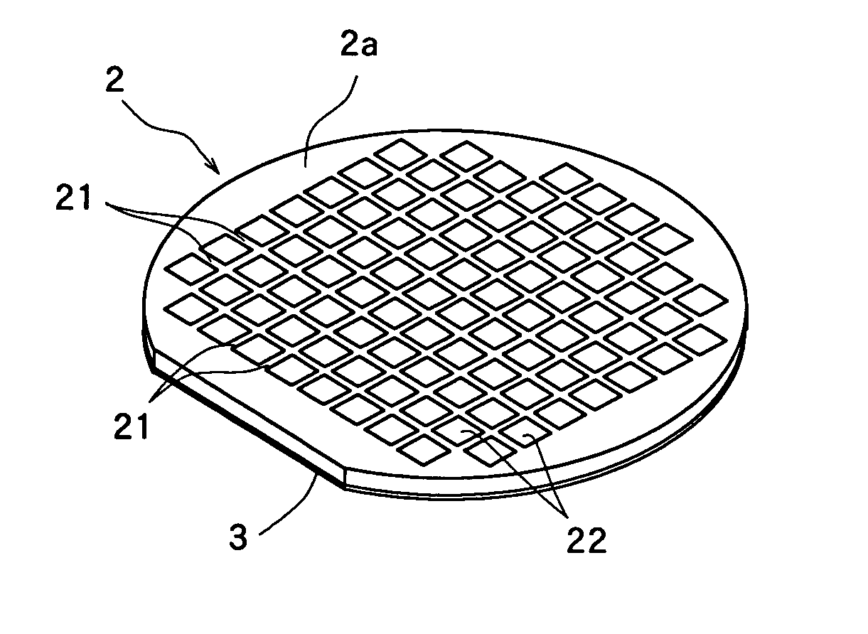
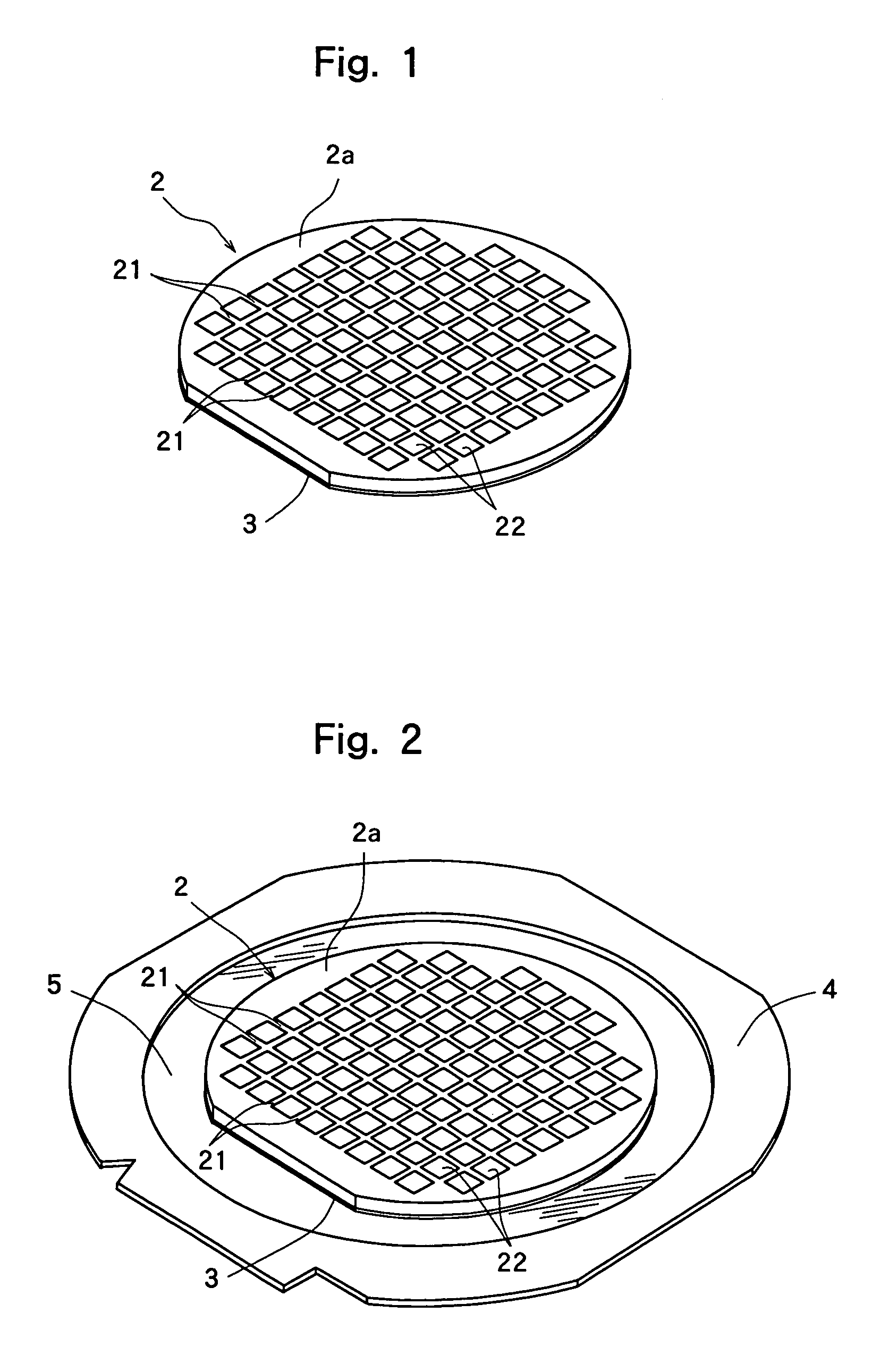
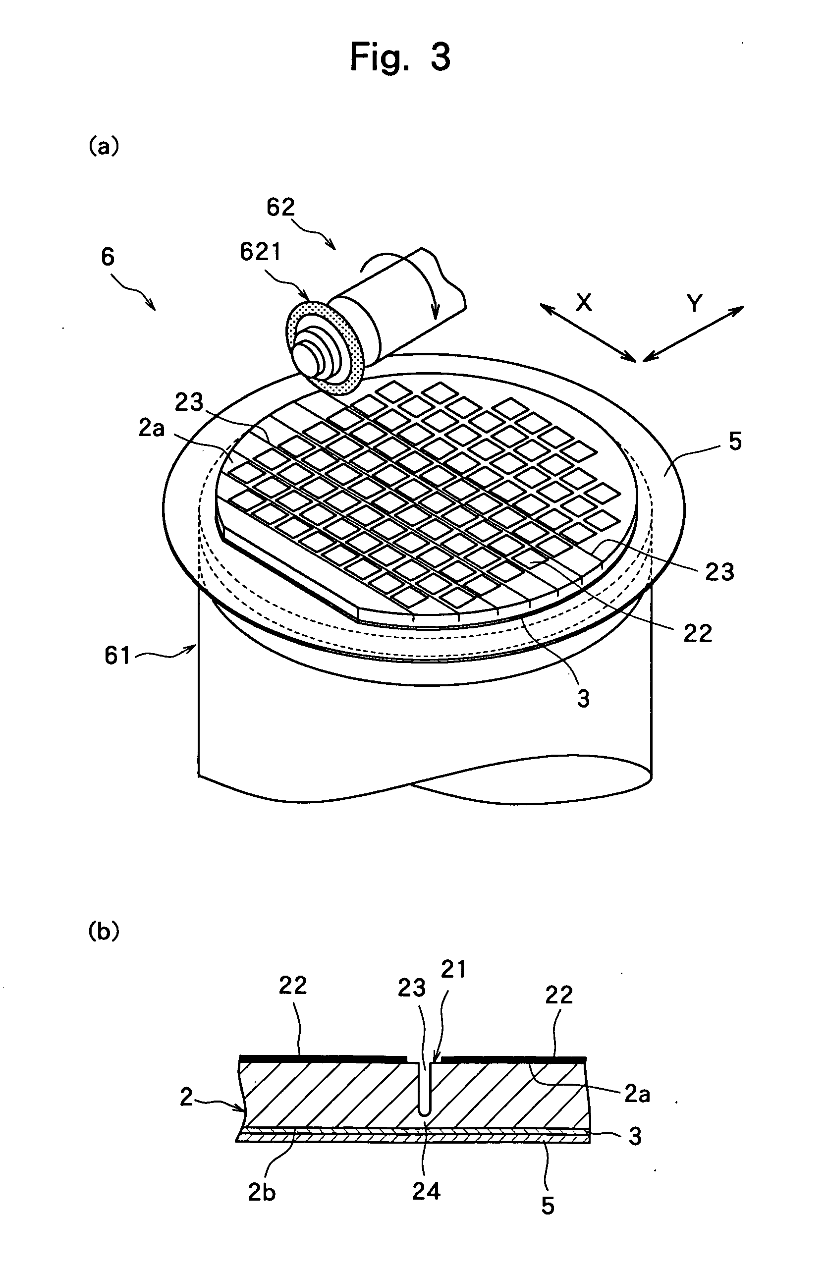
[0017]FIG. 1 is a perspective view of a semiconductor wafer to be divided according to the present invention. In the semiconductor wafer 2 shown in FIG. 1, a plurality of streets 21 are formed in a lattice pattern on the front surface 2a of a silicon substrate having a thickness of, for example, 600 μm and a device 22 such as a circuit is formed in each of a plurality of areas sectioned by the plurality of streets 21. The back surface 2b of the semiconductor wafer 2 is coated with a metal film 3 such as a gold, silver or titanium film having a thickness of several tens of nm.

[0018] To divide the above semiconductor wafer 2 into individual semiconductor chips, a wafer supporting step of putting the metal film 3 side of the semiconductor wafer 2 having the metal film 3 formed on the back surface 2b, on a dicing tape mounted on an annular frame is carried o...


PUM


Abstract

A method of dividing a wafer having a plurality of streets formed on the front surface in a lattice pattern, devices formed in a plurality of areas sectioned by the plurality of streets, and a metal film formed on the back surface, into individual chips, comprising: a street cutting step for cutting the front surface of the wafer along the streets to form grooves, leaving an uncut portion having a predetermined thickness on the back surface side; and a cutting-off step for cutting off the uncut portion and the metal film by applying a laser beam to the uncut portion of the groove formed along the streets.

Description

FIELD OF THE INVENTION [0001] The present invention relates to a method of dividing a wafer having a plurality of streets formed in a lattice pattern on the front surface, circuits formed in a plurality of areas sectioned by the plurality of streets and a metal film formed on the back surface, into individual chips. DESCRIPTION OF THE PRIOR ART [0002] In the production process of a semiconductor device, for example, individual semiconductor chips are manufactured by forming a circuit such as IC or LSI in a plurality of areas sectioned by cutting lines called “streets” formed in a lattice pattern on the front surface of a substantially disk-like semiconductor wafer and cutting the semiconductor wafer into the areas having the circuit formed thereon, along the streets. A cutting machine as disclosed by JP-A 2001-85365 is generally used as the dividing machine for dividing the semiconductor wafer. This cutting machine cuts the semiconductor wafer along the streets with a cutting blade ...

Claims


Application Information

Patent Timeline
IPC IPC(8): G03B7/26
CPCH01L21/78
Inventor GENDA, SATOSHI
Owner DISCO CORP
Why Eureka
Try Eureka