Interconnection architecture and method of assessing interconnection architecture

a technology of interconnection architecture and interconnection structure, applied in the direction of architecture with multiple processing units, general purpose stored program computers, instruments, etc., can solve the problems of limiting the performance factor of the connection length between cells, wasting other routing resources, and unable to solve the problem

Inactive Publication Date: 2006-03-09
RGT UNIV OF CALIFORNIA
View PDF7 Cites 20 Cited by
  • Summary
  • Abstract
  • Description
  • Claims
  • Application Information

AI Technical Summary

Problems solved by technology

Length of connection between cells is a limiting performance factor in terms of power consumption and latency, among other factors.
Unreasonable distribution of interconnect resources results in bottlenecks that stall data flow, whil

Method used


Image

  • Interconnection architecture and method of assessing interconnection architecture
  • Interconnection architecture and method of assessing interconnection architecture
  • Interconnection architecture and method of assessing interconnection architecture

Examples


Embodiment Construction

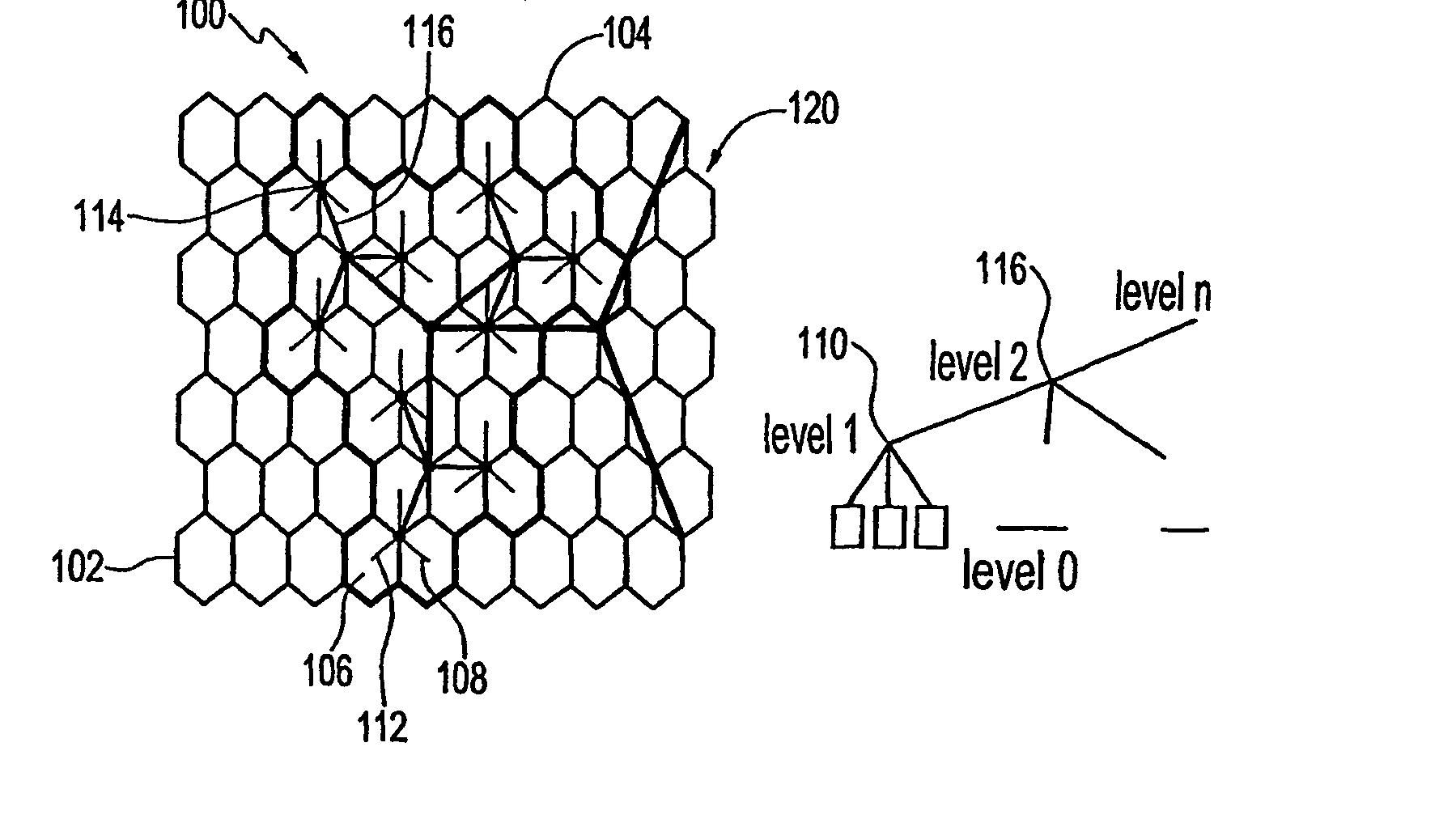
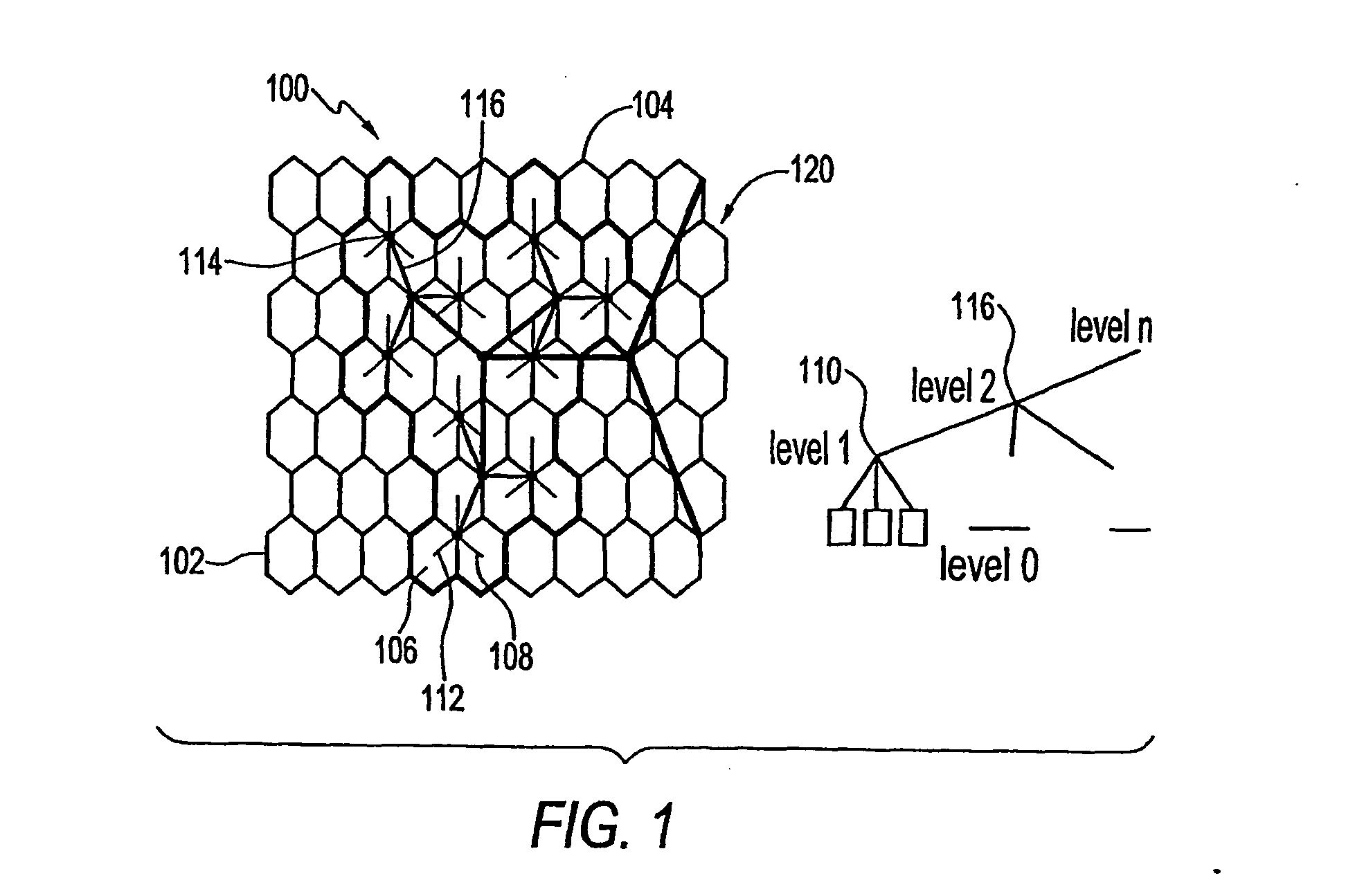
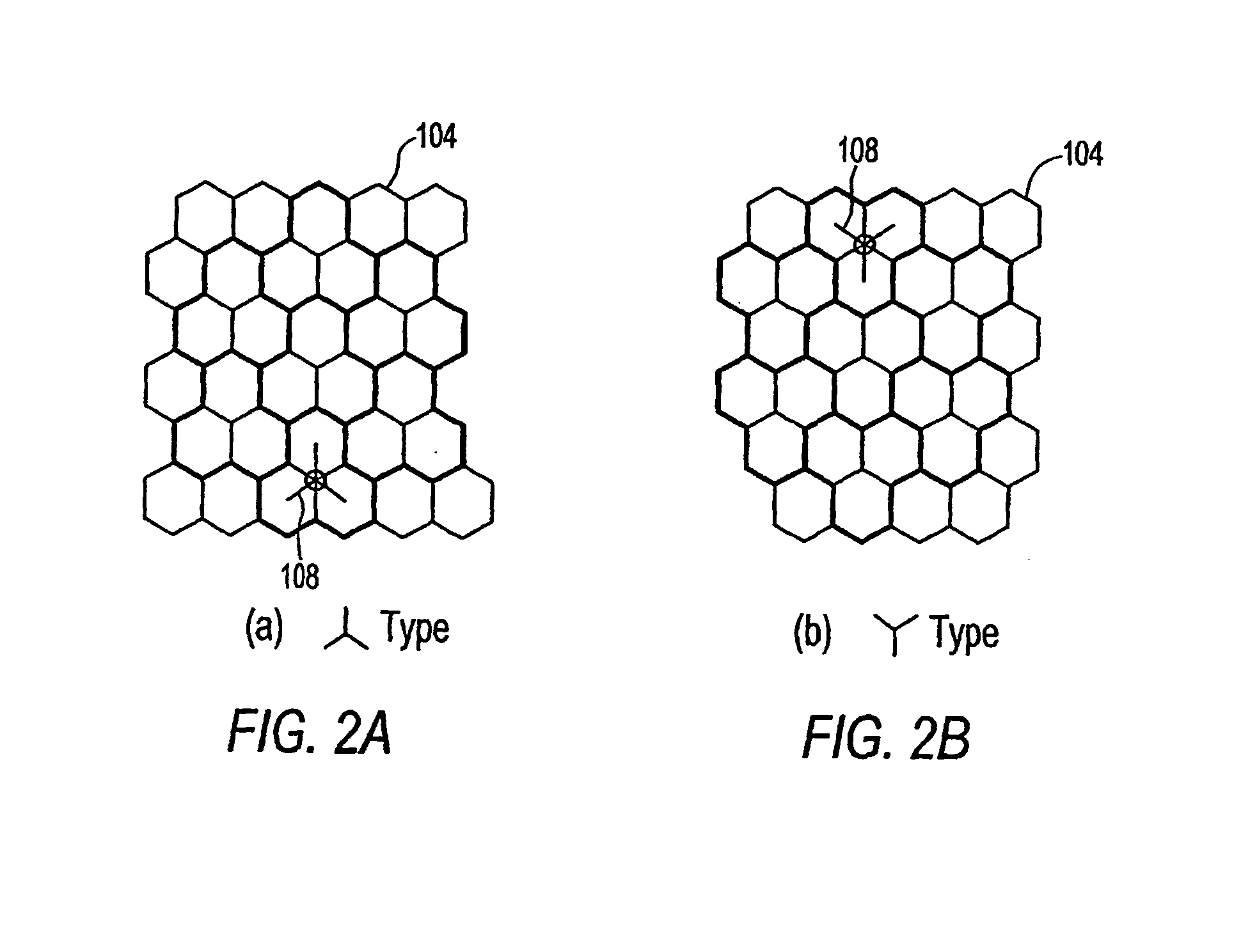
[0090] Interconnections among the cell array reveal themselves as a key problem, as the interconnect becomes one of the most precious resources on a chip. With the advent of deep sub-micron technologies, switches are becoming less costly, yet interconnects such as wires are still expensive. Therefore, optimization efforts according to embodiments of the present invention focus on the interconnect resources.

[0091] Traditional Manhattan interconnect architecture organizes interconnects on two orthogonal routing directions, 0° and 90°, for the simplicity of routing embedding and design rule checking. However, this artificial restriction on routing directions adds significant interconnect length compared with the Euclidean optimum, and thus decreases the communication capability of the on-chip interconnects.

[0092] One goal of certain embodiments of the present invention is to allocate channel capacities in a mesh routing architecture to improve, or maximize, its communication capabili...


PUM


Abstract

A multi-celled chip. The chip includes a plurality of hexagonal cells arranged in an array. A plurality of interconnects including Y's connect the cells in clusters of three cells each, so that each of the cells is interconnected.

Description

TECHNICAL FIELD [0001] The present invention relates generally to the field of chip design and fabrication. The present invention also relates generally to the field of circuit routing. BACKGROUND ART [0002] With submicron technology, large numbers of processors, elements, or devices can be integrated on microcircuit chips. The processors, elements, or devices are arranged in arrays of cells on one or more layers of a chip. Each of the cells, containing a component of one or more overall circuits, contains one or more terminals for communicating with other cells. To permit the cells to communicate with one another interconnects, such as routing wires or other conductive paths, connect the cells and / or bus segments, which themselves interconnect groups of cells. [0003] The interconnects are arranged in meshes formed in or among one or more interconnect layers (also known as routing layers) of a microcircuit chip. A mesh is a common routing architecture for many reconfigurable computi...

Claims


Application Information

Patent Timeline
IPC IPC(8): H01L29/76G06F15/80G06F17/50H01L23/528
CPCG06F15/8023G06F17/5077H01L23/528H01L27/0203H01L2924/0002H01L2924/00G06F30/394
Inventor CHENG, CHUNG-KUANCHEN, HONGGYYAO, BOGRAHAM, RONALDCHENG, ESTHERYZHOU, FENG
Owner RGT UNIV OF CALIFORNIA
Why Eureka
Try Eureka