Display device, method for manufacturing the same and apparatus for manufacturing the same

a display device and display technology, applied in the manufacture of electrode systems, electric discharge tubes/lamps, discharge tubes luminescent screens, etc., can solve the problems of insufficient crystallization of semiconductor films, limited manufacturing conditions, and film-type display devices that can be bent themselves, etc., to achieve excellent characteristics, low cost, and efficient manufacturing

Inactive Publication Date: 2006-03-16
SEMICON ENERGY LAB CO LTD
View PDF38 Cites 78 Cited by
  • Summary
  • Abstract
  • Description
  • Claims
  • Application Information

AI Technical Summary

Benefits of technology

[0018] By utilizing the apparatus for manufacturing a display device according to the present invention, a display device provided over a flexible substrate can be manufactured efficien

Problems solved by technology

Also, film-type display devices that can be bent themselves have been attracting attention, recently.
However, when a film-type display device is manufactured by directly forming a metal material or an insulating material over a flexible substrate made from plastic or the like, manufacturing conditions are limited due to a heat resistance property of the substrate and the like.
For example, in the case of forming pixels, driver circuits and the like of a display device are formed using thin film transistors (TFTs), conditions of a heat treatment and the like are limited so that a semiconductor film cannot be crystallized sufficient

Method used


Image

  • Display device, method for manufacturing the same and apparatus for manufacturing the same
  • Display device, method for manufacturing the same and apparatus for manufacturing the same
  • Display device, method for manufacturing the same and apparatus for manufacturing the same

Examples


embodiment mode 1

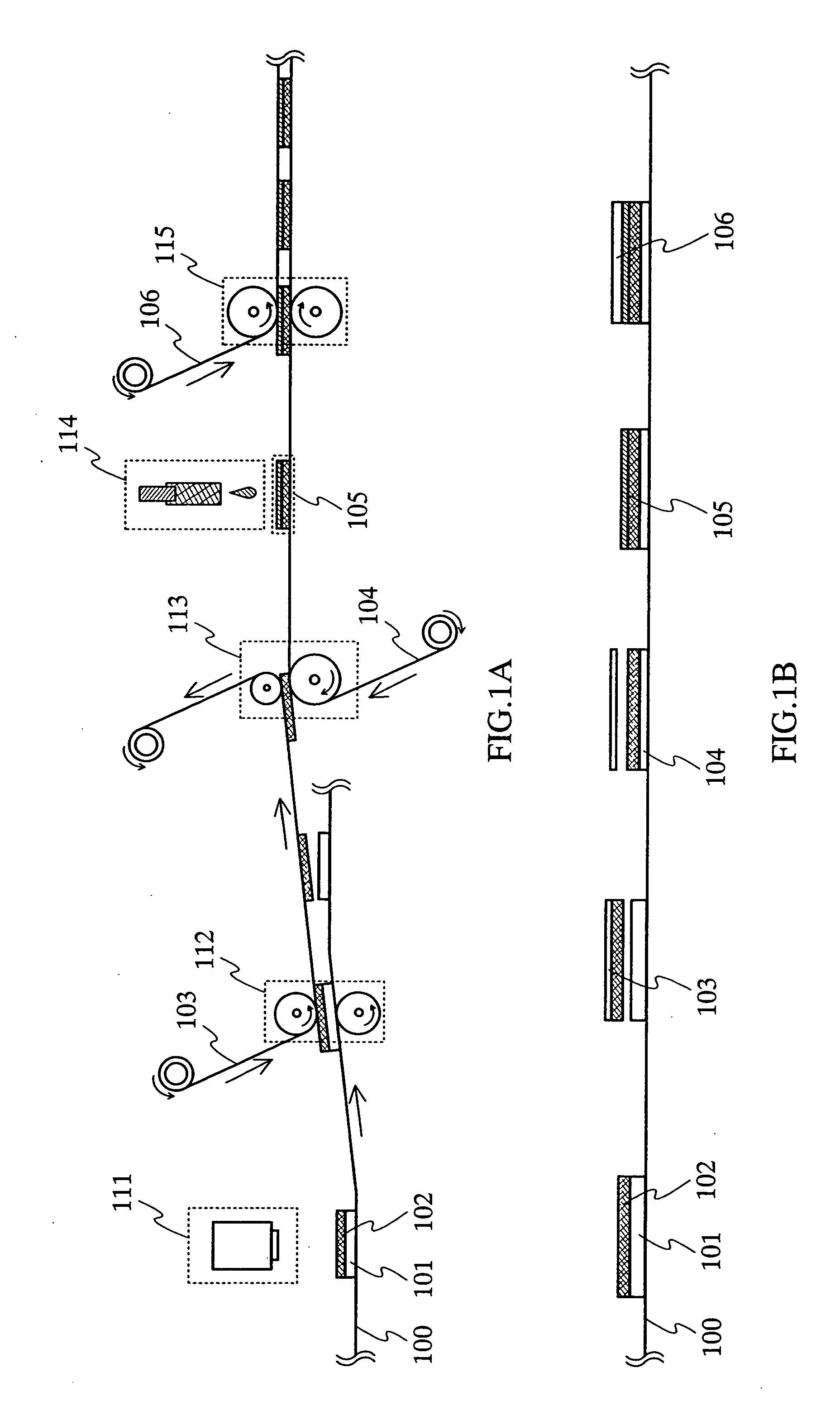
[0052] In Embodiment Mode 1, a more specific structure of the apparatus for manufacturing a display device as shown in FIG. 1A will be described with reference to the drawings.

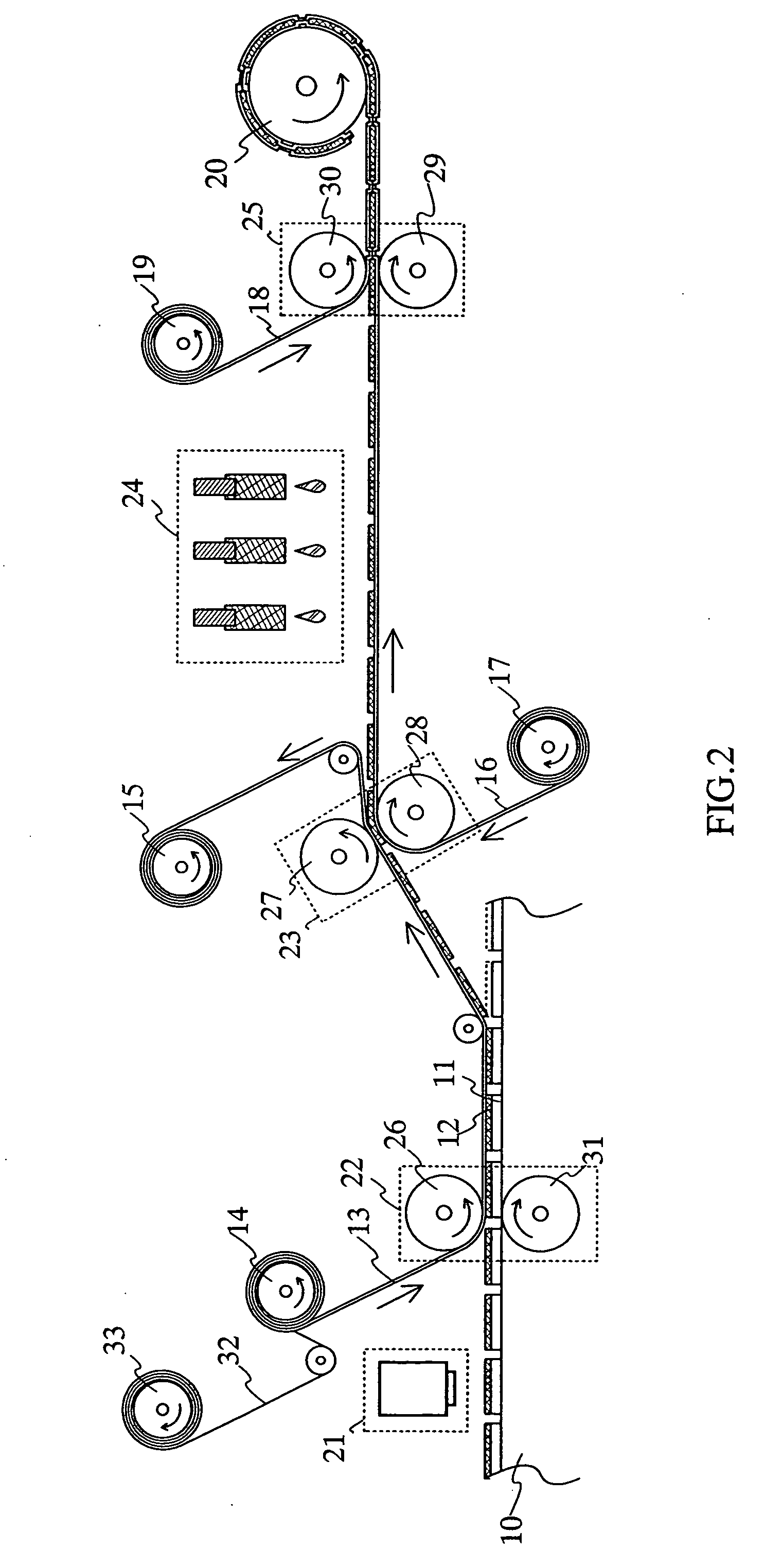
[0053] As shown in FIG. 2, an apparatus of Embodiment Mode 1 comprises transferring means 10 for transferring a substrate 11 over which an element formation portion 12 constituting a part of the display device (hereinafter referred to as the element formation portion 12) is provided; controlling means 21 for controlling a position of the substrate 11; a first supply roll 14 to which a first sheet material 13 is reeled; first separating means 22 including a roller 26 that is used for attaching the first sheet material 13 to the element formation portion 12 and separating the element formation portion from the substrate 11; a second supply roll 17 to which a second sheet material 16 is reeled; second separating means 23 including rollers 27 and 28 that are used for attaching the second sheet material 16 to the ...

embodiment mode 2

[0089] Next, a specific example of a method for manufacturing a display device will be described with reference to the drawings.

[0090] In this embodiment mode, some parts of a display device are formed in advance over a heat-resistant substrate such as glass. The parts of the display device formed over the substrate are separated form the substrate and then are attached to a flexible substrate. Remaining parts of the display device is then formed over the flexible substrate.

[0091] As shown in a schematic view of the display device of FIG. 5A, a pixel region 402 including a plurality of pixel portions, driver circuits 403 and 404 for driving the pixel portions are generally provided over a substrate 200 such as a glass substrate. In addition, a circuit for controlling the pixel portions is provided over the substrate 200 or outside of the substrate 200 while being electrically connected to the pixel portions.

[0092] In this embodiment mode, after forming some parts of a structure o...

embodiment mode 3

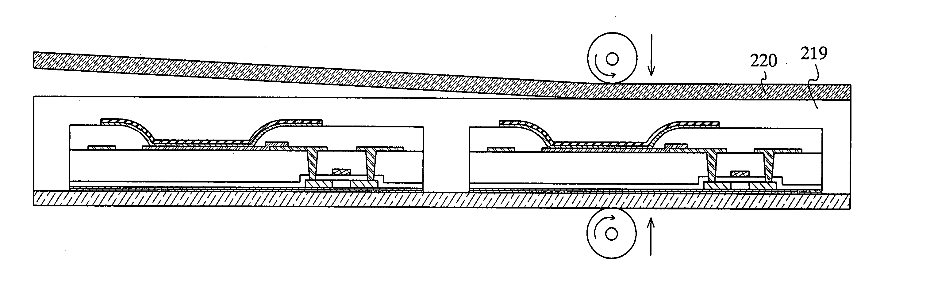
[0131] In this embodiment mode, a method for manufacturing a display device that is different from that of Embodiment Mode 2 will be described with reference to the drawings. Concretely, two kinds of methods for manufacturing display devices that are different from that of Embodiment Mode 2 will be described with reference to FIGS. 8A to 8D, FIGS. 9A to 9D, FIGS. 10A to 10D and FIGS. 11A to 11C. Further, same portions as those of Embodiment Mode 2 are denoted by same reference numerals.

[0132] In an example as shown in FIGS. 8A to 8D and FIGS. 9A to 9D, parts of a display device such as a separation layer 201, a first insulating film 202, a second insulating film 203, a semiconductor film 204 and a gate insulating film 205 are provided over a substrate 200. The parts of the display device are separated from the substrate. Thereafter, the parts of the display device separated from the substrate 200 are transferred to a flexible substrate. Remaining parts of the display device such as...


PUM


Abstract

The present inventions provides a method for manufacturing a film-type display device efficiently, and a method for manufacturing a large-size film-type display device, and an apparatus for manufacturing the film-type display device. An apparatus for manufacturing a film-type display device includes: transferring means for transferring a substrate over which an integrated circuit constituting the display device is provided; first separating means for separating the integrated circuit from the substrate by adhering a first sheet material to one surface of the integrated circuit; second separating means for separating the integrated circuit from the first sheet material by adhering a second sheet material to the other surface of the integrated circuit; processing means for forming one or both of a conductive film and an insulating film on the integrated circuit; and sealing means for sealing the processed integrated circuit with the second sheet material and a third sheet material.

Description

BACKGROUND OF THE INVENTION [0001] 1. Field of the Invention [0002] The present invention relates to a display device, a method for manufacturing the display device and an apparatus for manufacturing the display device. In particular, the invention relates to a display device formed over a flexible substrate that can be bent, a method for manufacturing thereof and an apparatus for manufacturing thereof. [0003] 2. Description of the Related Art [0004] In recent years, research and development of display devices using light emitting elements have been carried out actively. The display devices using the light emitting elements do not require backlights unlike display devices using liquid crystal and the like. Further, the display devices using the light emitting elements also have advantages of high viewing angle and the like. Also, film-type display devices that can be bent themselves have been attracting attention, recently. [0005] Methods for manufacturing the film-type display devi...

Claims


Application Information

Patent Timeline
IPC IPC(8): H05B33/08H05B33/10H05B44/00
CPCH01L51/0004H01L51/56H01L51/0024H10K71/13H10K71/50H10K71/00
Inventor NAKAMURA, OSAMUMORIYA, YOSHITAKA
Owner SEMICON ENERGY LAB CO LTD
Why Eureka
Try Eureka