METHOD TO BUILD SELF-ALIGNED NPN IN ADVANCED BiCMOS TECHNOLOGY

a technology of bicmos and self-alignment, applied in the direction of semi-conductor devices, basic electric elements, electrical equipment, etc., can solve the problems of serious device operation limitations

Active Publication Date: 2006-03-23
TAIWAN SEMICON MFG CO LTD
View PDF9 Cites 10 Cited by
  • Summary
  • Abstract
  • Description
  • Claims
  • Application Information

AI Technical Summary

Benefits of technology

[0017] In one embodiment of the present invention, the pedestal is an oxide pedestal. In this embodiment of the present invention, the low temperature process converts the polycrystalline material of the extra base layer atop the oxide pedestal into an oxide. During the subsequent removal process, the oxide produced by the low-temperature oxidation step and the oxide pedestal are removed in a single etching step. After removal of oxide, a second low temperature oxidation step is performed to provide at least an oxide layer within the emitter opening. A nitride spacer is then formed on each sidewall of the emitter opening and a chemical oxide removal (COR) process is employed to remove the oxide layer from the bottom of the emitter opening prior to forming the polysilicon emitter.
[0018] In one preferred embodiment of the present invention, the low temperature oxidation pro

Problems solved by technology

As the vertical dimensions of the bipolar transistor are scaled more a

Method used


Image

  • METHOD TO BUILD SELF-ALIGNED NPN IN ADVANCED BiCMOS TECHNOLOGY
  • METHOD TO BUILD SELF-ALIGNED NPN IN ADVANCED BiCMOS TECHNOLOGY
  • METHOD TO BUILD SELF-ALIGNED NPN IN ADVANCED BiCMOS TECHNOLOGY

Examples


Embodiment Construction

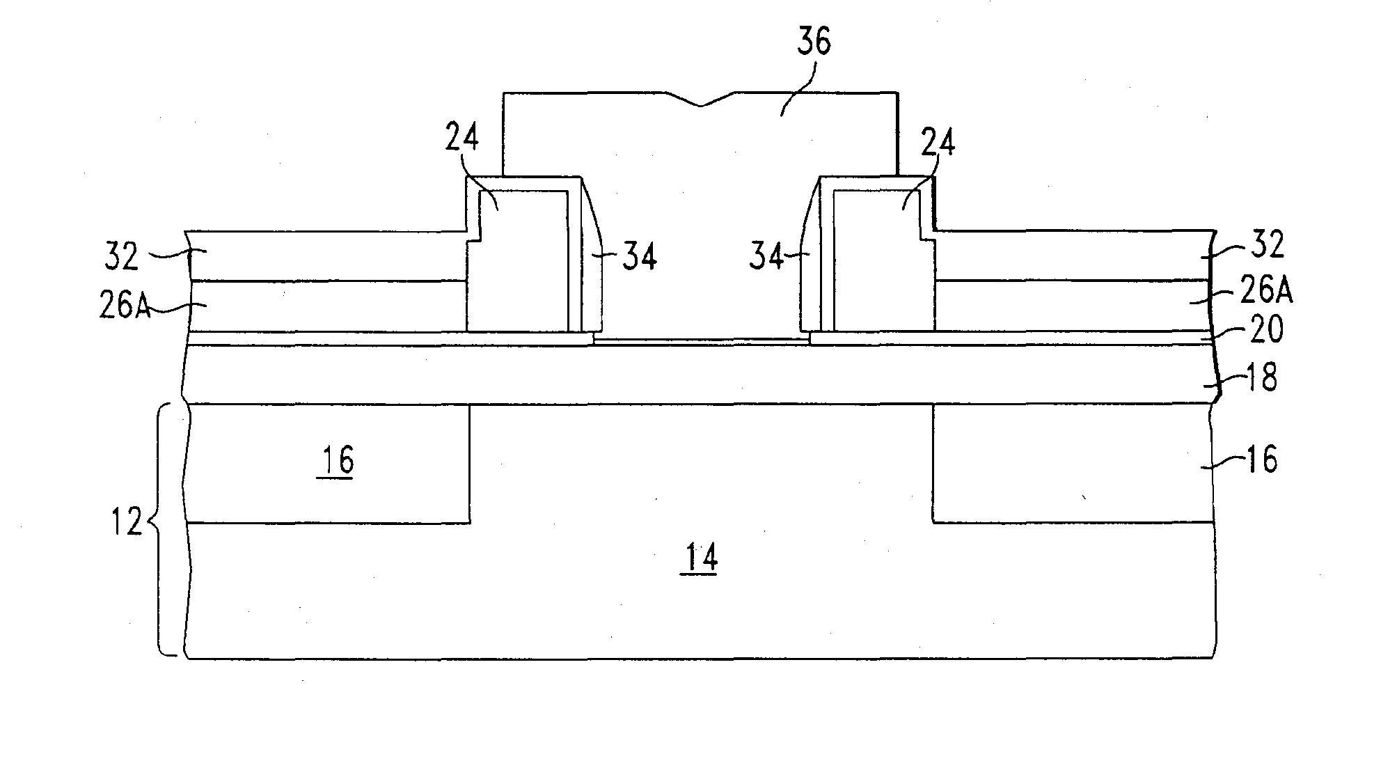
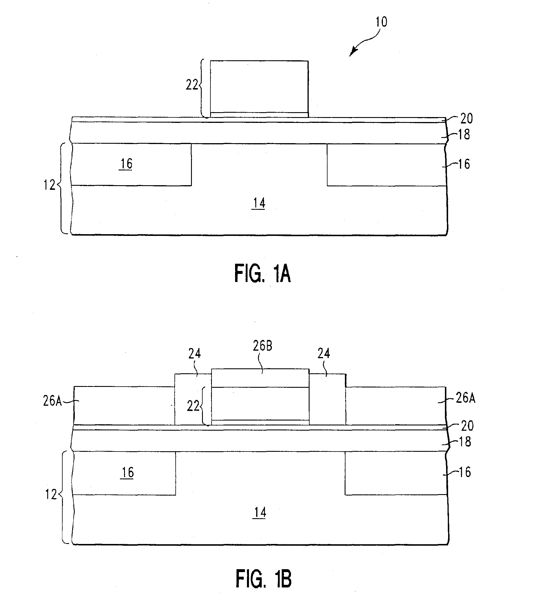
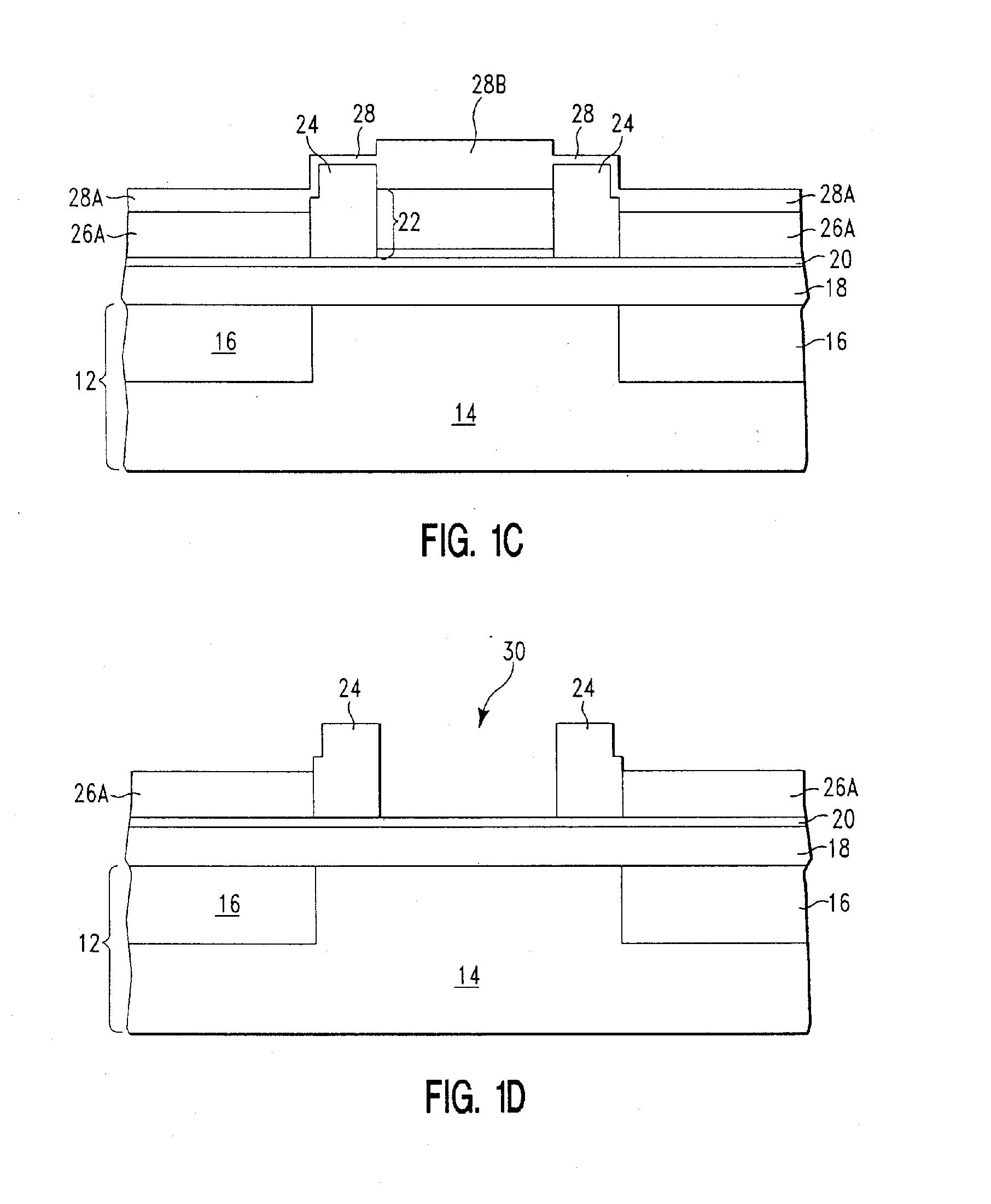
[0022] The present invention, which provides a method to build self-aligned HBT devices in advanced BiCMOS technology, will now be described in greater detail by referring to the drawings that accompany the present application. It is noted that the drawings are provided for illustrative purposes and are thus not drawn to scale. Moreover, in the drawings, like and corresponding elements are referred to by like reference numerals.

[0023] The drawings of the present application are directed to the HBT device area only. For clarity, the CMOS device area as well as the other areas of a typically BiCMOS structure are not shown in the drawings of the present application. The other areas including the CMOS device area lay to the periphery of the HBT device area shown. Also, despite showing the presence of a single HBT device area, the present invention also can be employed in fabricating HBT devices in a plurality of HBT device areas. The CMOS device areas can be formed before or after comp...


PUM


Abstract

The present invention provides a method of forming a self-aligned heterobipolar transistor (HBT) device in a BiCMOS technology. The method includes forming a raised extrinsic base structure by using an epitaxial growth process in which the growth rate between single crystal silicon and polycrystalline silicon is different and by using a low temperature oxidation process such as a high-pressure oxidation (HIPOX) process to form a self-aligned emitter/extrinsic base HBT structure.

Description

FIELD OF THE INVENTION [0001] The present invention relates to heterojunction bipolar transistors (HBTs) and more particularly to a method of forming a self-aligned HBT device for use in advanced bipolar and complementary metal oxide semiconductor (BiCMOS) technology. The method provides a self-aligned HBT having a high unity gain frequency fT that is greater than 200 GHz. BACKGROUND OF THE INVENTION [0002] Bipolar transistors are electronic devices with two p-n junctions that are in close proximity to each other. A typical bipolar transistor has three device regions: an emitter, a collector, and a base disposed between the emitter and the collector. Ideally, the two p-n junctions, i.e., the emitter-base and collector-base junctions, are in a single layer of semiconductor material separated by a specific distance. Modulation of the current flow in one p-n junction by changing the bias of the nearby junction is called “bipolar-transistor action.”[0003] If the emitter and collector ar...

Claims


Application Information

Patent Timeline
IPC IPC(8): H01L29/737H01L21/331
CPCH01L29/7378H01L29/66242
Inventor DUNN, JAMES S.JOSEPH, ALVIN J.LIU, QIZHI
Owner TAIWAN SEMICON MFG CO LTD
Why Eureka
Try Eureka