Semiconductor device with improved heat dissipation, and a method of making semiconductor device

a semiconductor device and heat dissipation technology, applied in semiconductor devices, semiconductor/solid-state device details, electrical devices, etc., can solve the problem of inefficient heat dissipation from the semiconductor chip b>2/b> to the heat dissipation member b>4/b>, and achieve the effect of simplifying the method of making the semiconductor devi

Inactive Publication Date: 2006-03-30
FUJITSU LTD
View PDF16 Cites 8 Cited by
  • Summary
  • Abstract
  • Description
  • Claims
  • Application Information

AI Technical Summary

Benefits of technology

[0025] In the invention described above, a stress generated between the semiconductor chip and the heat dissipation member is absorbed by the coupling member, so that the stress applied to the semiconductor chip is reduced, thereby improving the reliability of the semiconductor device. Further, metal-metal bonding between the coupling member and the semiconductor chip enhances thermal conductivity between the coupling member and the semiconductor chip, which achieves efficient heat dissipation with respect to heat generated by the semiconductor chip.
[0029] In the invention described above, the deformable posts can reliably absorb a stress generated between the semiconductor chip and the heat dissipation member.
[0031] In the invention described above, the organic material filling the gaps between the posts reinforces the joints between the coupling member and the semiconductor chip, thereby improving the reliability of joints between the coupling member and the semiconductor chip.
[0033] In the invention described above, the inclusion of the inorganic material provides a coefficient of thermal expansion between that of the semiconductor chip and that of the heat dissipation member, thereby reducing a stress that is applied to the semiconductor chip by the organic material.
[0035] In the invention described above, the coupling member has higher rigidity near the center where a smaller stress is generated, and has lower rigidity to provide elasticity near the perimeter where a larger stress is generated. In this manner, the posts are given elasticity commensurate with the strength of a stress, thereby reliably absorbing the stress generated between the semiconductor chip and the heat dissipation member in an efficient manner.
[0039] In the invention described above, the process of joining the posts to the metal layer and the process of filling the gaps between the posts with the resin material are simultaneously performed, thereby simplifying the method of making the semiconductor device.

Problems solved by technology

In the scheme (a) described above, either grease (compound) or a heat conductive adhesive has high thermal resistance, giving rise to a problem in that thermal conduction from the semiconductor chip 2 to the heat dissipation member 4 is not efficiently carried out.

Method used


Image

  • Semiconductor device with improved heat dissipation, and a method of making semiconductor device
  • Semiconductor device with improved heat dissipation, and a method of making semiconductor device
  • Semiconductor device with improved heat dissipation, and a method of making semiconductor device

Examples


first embodiment

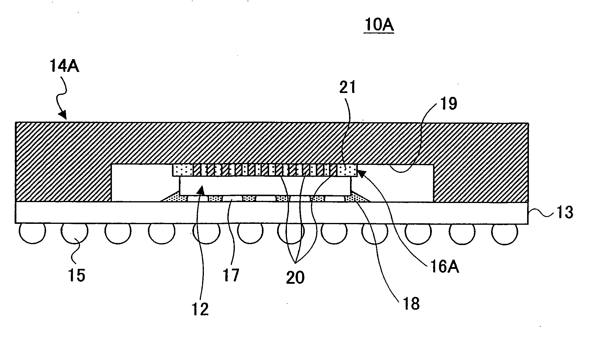
[0053]FIG. 2 is an illustrative drawing showing a semiconductor device 10A according to the invention. The semiconductor device 10A shown in FIG. 2 has an FC-BGA structure, and schematically includes a semiconductor chip 12, a package substrate 13, a heat dissipation member 14A, solder balls 15, and a coupling member 16A.

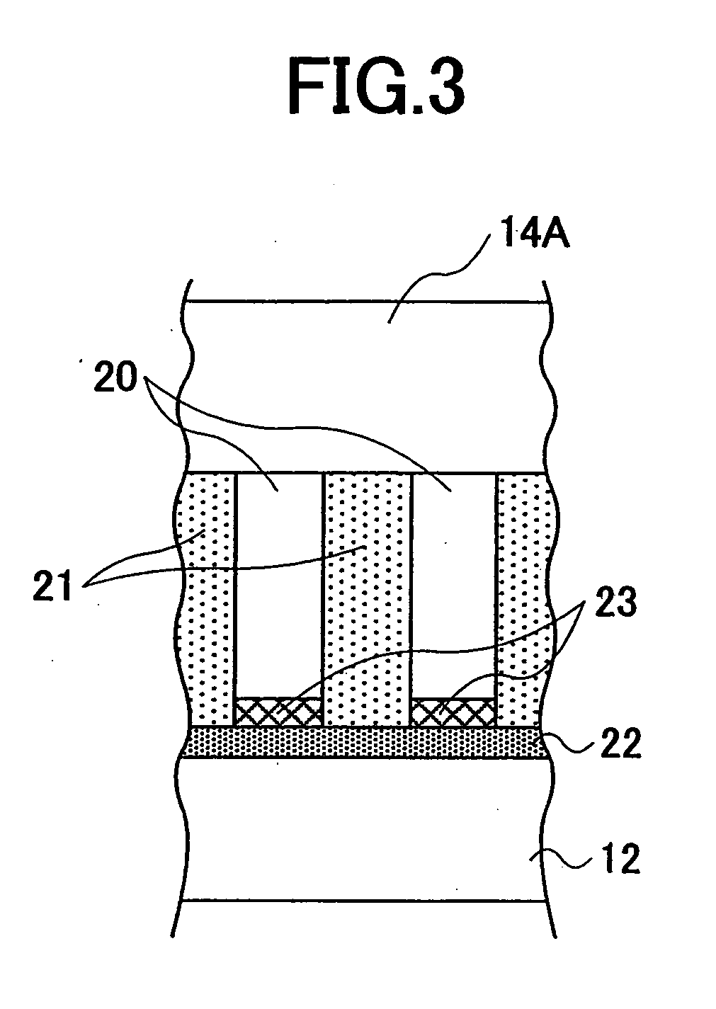
[0054] The semiconductor chip 12 is mounted through flip-chip implementation by use of bumps 17 on the upper surface of the package substrate 13. Between this semiconductor chip 12 and the package substrate 13, underfill resin 18 is provided in order to prevent the stress resulting from different thermal expansion between the semiconductor chip 12 and the package substrate 13 from being concentrated on the bumps 17. Moreover, as shown in an expanded view of FIG. 3, a metal layer 22 is formed on the back surface of the semiconductor chip 12. Posts 20, which will be later described, are connected to the metal layer 22 through a joint material 23.

[0055] The solder bal...

third embodiment

[0091]FIG. 8 is an illustrative drawing showing the semiconductor device 10C according to the The semiconductor device 10C according to this embodiment is characterized in that the posts 20 constituting a coupling member 16C have different heights. Specifically, steps 37 are formed on a heat dissipation member 14C, so that the lengths of the posts 20 near the center (the length of a post 20b situated at the center is shown by an arrow Hb) are shorter than the lengths of the posts 20 near the perimeter (the length of a post 20a situated at the perimeter is shown by an arrow Ha) That is, Ha>Hb.

[0092]FIG. 9 is an illustrative drawing showing the semiconductor device 10D according to the fourth embodiment. Like the semiconductor device 10C of the third embodiment, the semiconductor device 10D of the fourth embodiment has the posts 20 constituting a coupling member 16D and having different heights.

[0093] Specifically, a spherical member 38 is formed on a heat dissipation member 14D, so...

fifth embodiment

[0094]FIG. 10 is an illustrative drawing showing the semiconductor device 10E according to the The semiconductor device 10E according to this embodiment is characterized in that the posts 20 constituting a coupling member 16E have different cross-sectional areas.

[0095] Specifically, the cross-sectional areas of the posts 20 near the center (the cross-sectional area of a post 20b situated at the center is represented by Sb) are larger than the cross-sectional areas of the posts 20 near the perimeter (the cross-sectional area of a post 20a situated at the perimeter is represented by Sa). That is, Sa20 may be gradual from the center toward the perimeter, or may be stepwise.


PUM


Abstract

A semiconductor device includes a semiconductor chip, a heat dissipation member for dissipating heat generated by the semiconductor chip, and a coupling member which thermally couples the semiconductor chip to the heat dissipation member, wherein the coupling member is made of metal and deformable to absorb a stress generated between the semiconductor chip and the heat dissipation member, the coupling member and the semiconductor chip being joined through metal-metal bonding.

Description

CROSS-REFERENCE TO RELATED APPLICATIONS [0001] The present application is based upon and claims the benefit of priority from the prior Japanese Patent Application No. 2003-044335 filed on Feb. 21, 2003, with the Japanese Patent Office, the entire contents of which are incorporated herein by reference. BACKGROUND OF THE INVENTION [0002] 1. Field of the Invention [0003] The present invention generally relates to semiconductor devices and methods of making the semiconductor devices, and particularly relates to a semiconductor device and a method of making the semiconductor device in which the efficiency of heat dissipation regarding heat generated by a semiconductor chip is improved. [0004] 2. Description of the Related Art [0005] In recent years, the circuit integration of semiconductor chips has been further enhanced, and there has been a demand for higher density for the implementation of semiconductor devices. Against this background, BGA-type semiconductor devices and LGA-type sem...

Claims


Application Information

Patent Timeline
Patent Type & Authority Applications(United States)
IPC IPC(8): H01L21/48H01L23/34H01L23/36H01L23/373H01L23/433
CPCH01L23/3737H01L2224/32245H01L24/32H01L2224/16225H01L2224/16227H01L2224/73204H01L2224/73253H01L2924/01004H01L2924/01005H01L2924/01013H01L2924/01029H01L2924/01033H01L2924/0105H01L2924/01051H01L2924/01074H01L2924/01075H01L2924/01078H01L2924/01079H01L2924/01082H01L2924/12044H01L2924/15153H01L2924/1517H01L2924/15311H01L2924/16152H01L2924/16195H01L21/4871H01L21/4882H01L23/36H01L23/3677H01L23/3733H01L2924/0132H01L2924/01006H01L2924/01019H01L23/433H01L2224/2919H01L2224/32225H01L2224/29111H01L2924/00H01L2924/00014H01L2224/2612H01L23/34
Inventor YOSHIMURA, HIDEAKI
Owner FUJITSU LTD
Why Eureka
Try Eureka