

Semiconductor light emitting device having narrow radiation spectrum
- Summary
- Abstract
- Description
- Claims
- Application Information
AI Technical Summary
Benefits of technology
Problems solved by technology
Method used
Image

Examples
Embodiment Construction
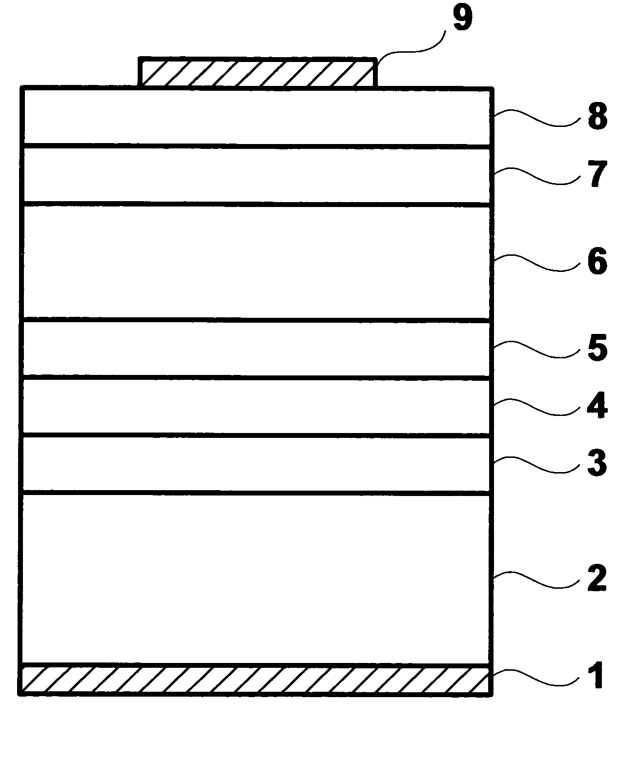
[0017]FIG. 1 is a schematic cross sectional view of a semiconductor light emitting device according to the first embodiment. On a principal surface of a semiconductor substrate 2 made of p-type GaAs, a lower clad layer 3, an active layer 4, an upper clad layer 5, a current spreading layer 6, an optical absorption layer 7 and a contact layer 8 are laminated in this order from the bottom.
[0018] The lower clad layer 3 is made of Zn- or Mg-doped p-type AlGaAs and has a thickness of 1 to 3 μm. A composition ratio of Al of the lower clad layer 3 is 0.3 to 0.4 and an impurity concentration is 1×1016 cm−3 to 1×1018 cm−3. The active layer 4 is made of p-type GaAs and has a thickness of 50 to 500 nm. An impurity concentration of the active layer 4 is 1×1017 cm−3 to 5×1018 cm−3.
[0019] The upper clad layer 5 is made of Si- or Se-doped n-type AlGaAs and has a thickness of 1 to 3 μm. A composition ratio of Al of the upper clad layer 5 is 0.3 to 0.4 and an impurity concentration is about 1×10¹⁸ ...
PUM
 Abstract
Description
Claims
Application Information