Semiconductor laser device

a laser device and semiconductor technology, applied in semiconductor lasers, mechanical measuring arrangements, instruments, etc., can solve the problems of insufficient effect of semiconductor laser devices of the prior art to suppress ripples, ffp ripples, etc., to suppress ripples in the ffp of laser beams, less ripples, and less ripples.

Active Publication Date: 2006-04-13
NICHIA CORP
View PDF13 Cites 68 Cited by
  • Summary
  • Abstract
  • Description
  • Claims
  • Application Information

AI Technical Summary

Benefits of technology

[0007] An object of the present invention is to provide a semiconductor laser device that has a FFP with a Gaussian distribution so that it is less prone to ripples.

Problems solved by technology

When light leaks out of the waveguide region, stray light that has leaked escapes from an end face as weak light, that becomes noise superposed on the main beam, thus causing ripples in FFP.
Since such noise (ripples) causes various trouble when the laser is coupled to an optical fiber or a lens, there are demands for a semiconductor laser that has high output power and can form a FFP that is free of ripples.
However, the effect of the semiconductor laser device of the prior art to suppress ripples is not sufficient.

Method used


Image

  • Semiconductor laser device
  • Semiconductor laser device
  • Semiconductor laser device

Examples


embodiment 1

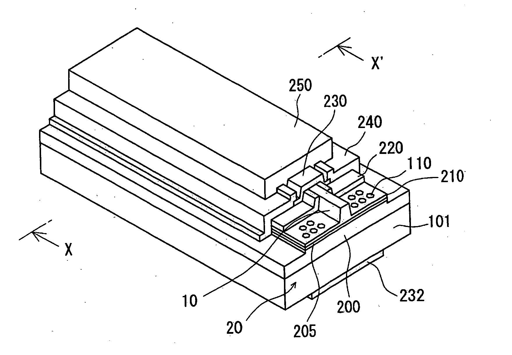
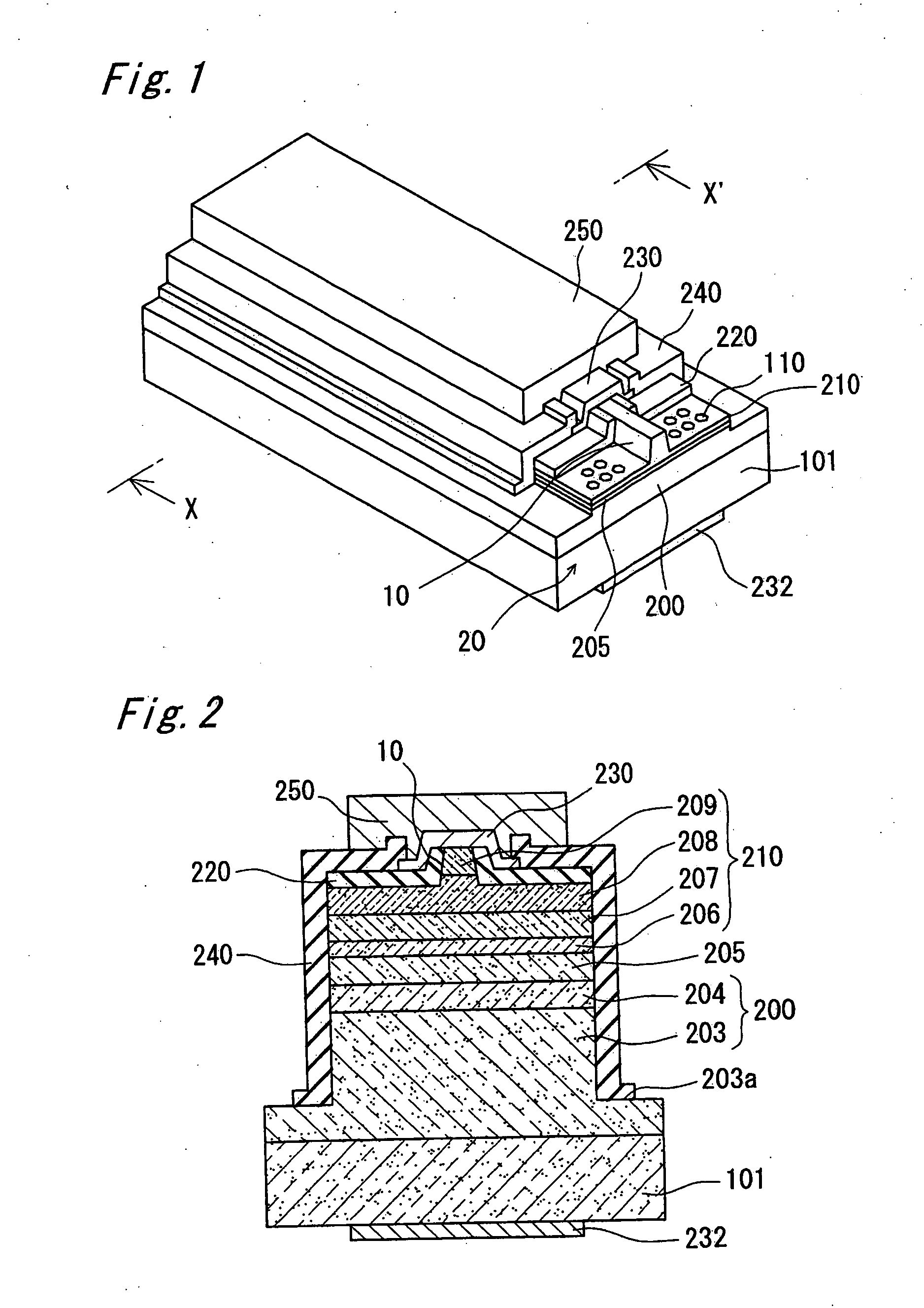
[0071]FIG. 1 is a schematic perspective view of a semiconductor laser device according to a first embodiment of the present invention. The semiconductor laser device comprises a nitride semiconductor layer 200 of a first conductivity type, an active layer 205 and a semiconductor layer 210 of a second conductivity type stacked on a first principal surface of a semiconductor substrate 101 that has the first principal surface and the second principal plane. The substrate 101 has electrical conductivity, and has an opposing electrode structure where electrodes are formed on the second principal surface of the substrate 101 and on the semiconductor layer 210 having the second conductivity type. The opposing electrode structure enables it to draw a large current which results in a high power oscillation. The semiconductor layer 210 of the second conductivity type has a ridge 10 of a stripe shape formed thereon, thus resulting in a waveguide region of stripe shape formed below the ridge 10...

embodiment 2

[0144] This embodiment makes it easier to cleave a wafer when forming the resonance surface by dividing the wafer into bars. The semiconductor laser of the present invention is similar to the semiconductor laser of the first embodiment except for the points described below.

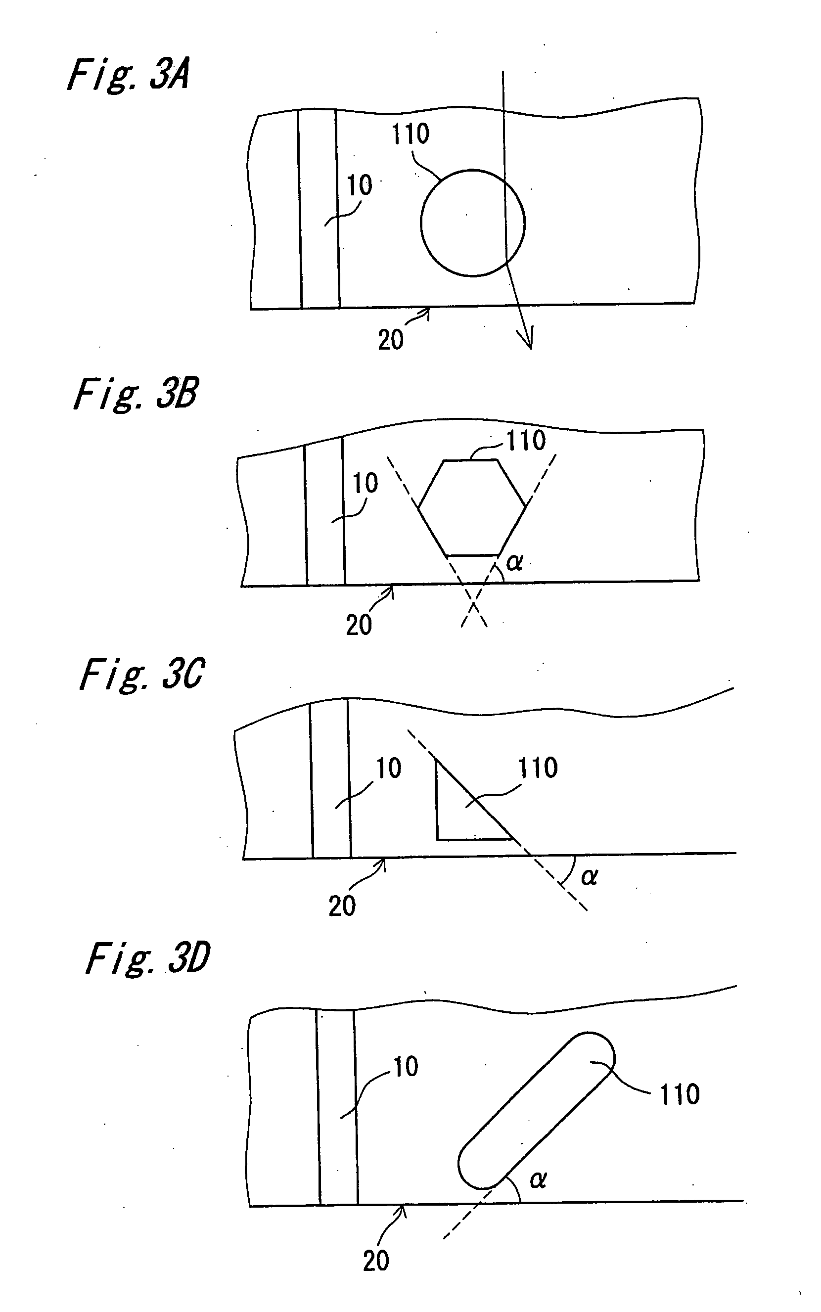
[0145]FIG. 8A is a perspective view of the semiconductor laser device of the second embodiment, and FIG. 8B is a partially enlarged perspective view of the recesses 110 shown in FIG. 8A. As shown in FIG. 8A and FIG. 8B, the semiconductor laser device of this embodiment has the arrangement of the recesses 110 so they overlap with the resonance surface 20, thereby having a notch formed in the resonance surface 20. This allows the recesses 110 that overlap the resonance surface 20 to function also as a cleavage assisting groove that assist to cleave the resonance surface 20, thus suppressing the occurrence of such a defect as deflection of the direction of cleaving.

[0146] In this embodiment, too, the recesses 110 c...

embodiment 3

[0154] The semiconductor laser device of this embodiment has both the p electrode 230 and the n electrode 232 formed on the first principal surface of the substrate 101. That is, the semiconductor layer 200 of the first conductivity type, the active layer 205 and the semiconductor layer 210 of the second conductivity type having a conductivity type different from that of the semiconductor layer 200 of the first conductivity type are stacked on the first principal surface of the substrate 101. The semiconductor layer 210 of the second conductivity type, the active layer 205 and a part of the semiconductor layer 200 of the first conductivity type are etched, thereby exposing the semiconductor layer 200 of the first conductivity type. The n electrode 232 is formed on the semiconductor layer 200 of the first conductivity type that is exposed. This embodiment is similar to the first embodiment in other regards. With the construction of this embodiment, the substrate is not limited to ele...


PUM


Abstract

A semiconductor laser device having a far field pattern (FFP) with a Gaussian distribution that is less prone to ripples is provided. The semiconductor laser device comprises a semiconductor layer having a first conductivity type, an active layer, a semiconductor layer having a second conductivity type, a waveguide region formed by restricting current within a stripe-shaped region in the semiconductor layer of the second conductive type, and a resonance surface provided on an end face substantially perpendicular to the waveguide region. A plurality of recesses is formed at positions spaced from the waveguide region in the semiconductor layer of the second conductivity type in a region adjacent to the resonance surface.

Description

1. FIELD OF THE INVENTION [0001] The present invention relates to a semiconductor laser device having a favorable far field pattern (hereinafter referred to as FFP). 2. DISCUSSION OF THE RELATED ART [0002] The semiconductor laser device of the present invention can be used in any apparatus, for example, an optical disk, an optical communication system, a printer or a measuring instrument. [0003] In a semiconductor laser, a striped structure is formed so as to control the transverse mode of light, thereby causing resonance of light in a waveguide region of the striped shape. When light leaks out of the waveguide region, stray light that has leaked escapes from an end face as weak light, that becomes noise superposed on the main beam, thus causing ripples in FFP. This phenomenon becomes conspicuous particularly in a semiconductor laser of high output power. Since such noise (ripples) causes various trouble when the laser is coupled to an optical fiber or a lens, there are demands for ...

Claims


Application Information

Patent Timeline
Patent Type & Authority Applications(United States)
IPC IPC(8): H01S5/00H01S5/02H01S5/024H01S5/16H01S5/20H01S5/22H01S5/32H01S5/343
CPCB82Y20/00H01S5/0202H01S5/0224H01S5/024H01S5/16H01S5/1017H01S5/22H01S5/3216H01S5/34333H01S2301/18H01S2304/12H01S5/2009H01S5/0234G01B3/10G01B5/02G01B5/18
Inventor MATSUMURA, HIROAKIKOTANI, YASUHISA
Owner NICHIA CORP
Why Eureka
Try Eureka