

Method of fabricating microneedles
a technology of microneedles and manufacturing methods, applied in the field of microneedles, can solve the problems of metal microneedles, high brittleness of silicon, and high cost of processing steps
- Summary
- Abstract
- Description
- Claims
- Application Information
AI Technical Summary
Problems solved by technology
Method used
Image

Examples
third embodiment
[0024]FIG. 4 is a flow chart illustrating a method for fabricating a microneedle in accordance with the present invention. In this embodiment, a substrate is provided at step 400. A metal-containing seed layer is formed on the substrate at step 401. A nonconductive pattern is formed on a portion of the seed layer at step 402. At step 403, a first metal layer is plated on the seed layer and over the edge of the nonconductive pattern to create a micromold with an opening. The micromold is separated from the seed layer and the nonconductive pattern at step 404. At step 405, a second metal is plated onto the micromold, thereby filling the opening and coating the exposed top and bottom surfaces of the micromold with the second metal. The micromold is selectively etched to release the plated second metal at step 406. The plated second metal from step 406 has the configuration of a microneedle structure attached to an excess layer. The microneedle structure is then separated from the exces...
fourth embodiment
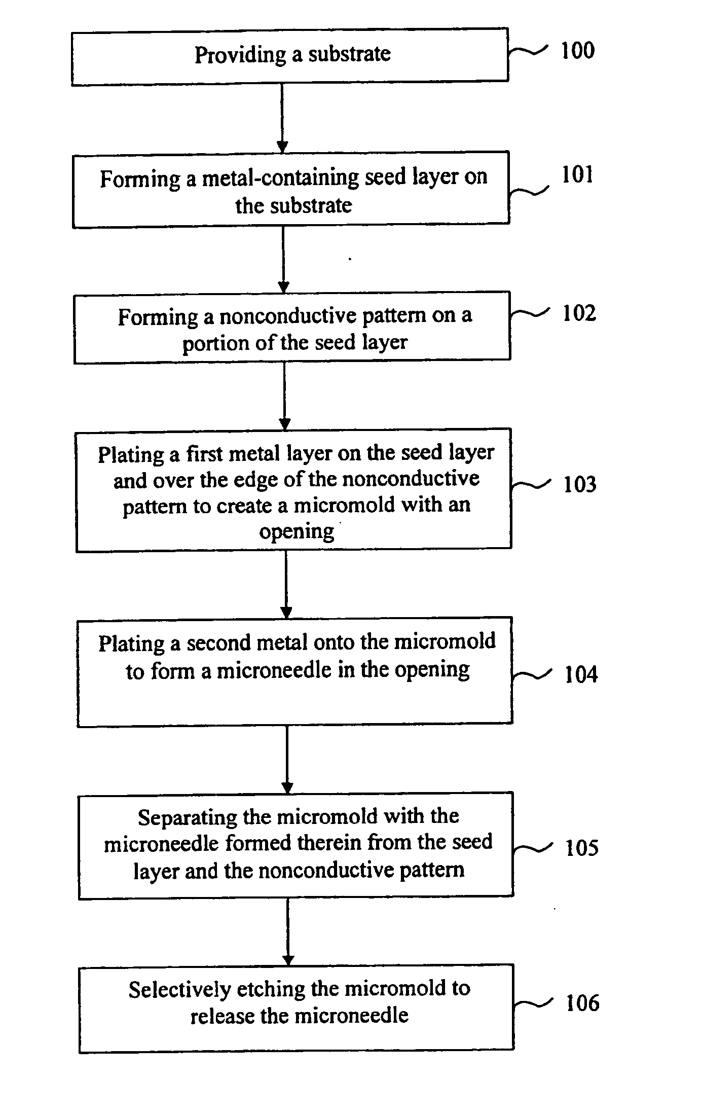
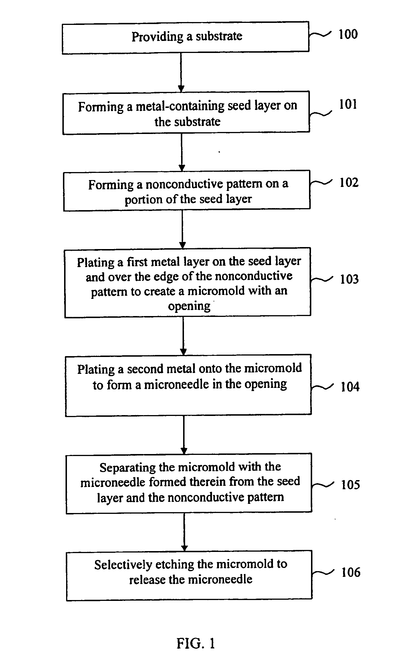
[0026]FIG. 6 is a flow chart illustrating the processing sequence for fabricating a microneedle with a sharp tip in accordance with the present invention. In this embodiment, a substrate having a recess in the top surface is provided at step 600. A metal-containing seed layer is formed on the top surface at step 601. A nonconductive pattern is formed on the seed layer at step 602 so that a portion of the nonconductive pattern is in the recess. At step 603, a first metal layer is plated on the seed layer and over the edge of the nonconductive pattern to create a micromold with an opening. Next, at step 604, a second metal is plated onto the micromold to form a microneedle in the opening. The micromold together with the microneedle formed therein are separated from the seed layer and the nonconductive pattern at step 605. The micromold is then selectively etched to release the microneedle at step 606.
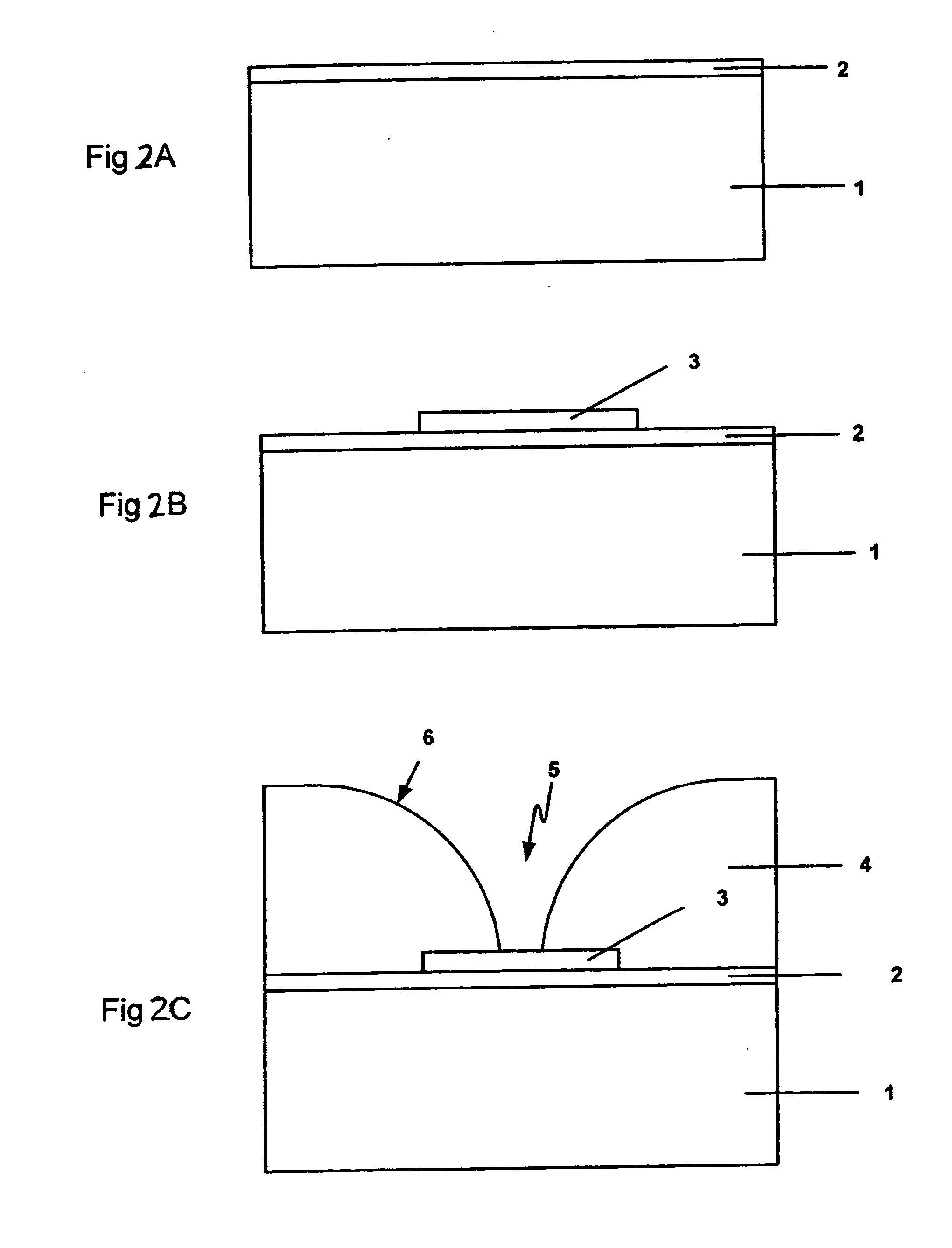
[0027]FIGS. 7A-7F show the cross-sectional views illustrating the method steps of FIG...
fifth embodiment
[0031]FIG. 8 is a flow chart illustrating the processing sequence for fabricating a microneedle with a slanted sharp tip in accordance with the present invention. In this embodiment, a substrate having a recess with an apex in the top surface is provided at step 800. A metal-containing seed layer is formed on the top surface at step 801. A nonconductive pattern is formed on the seed layer at step 802 so that a portion of the nonconductive pattern is in the recess. At step 803, a first metal layer is plated on the seed layer and over the edge of the nonconductive pattern to create a micromold with an opening that is laterally offset from the apex. Next, at step 804, a second metal is plated onto the micromold to form a microneedle in the opening. The micromold together with the microneedle formed therein are separated from the seed layer and the nonconductive pattern at step 805. The micromold is then selectively etched to release the microneedle at step 806.
[0032] Referring to FIG. ...
PUM
 Abstract
Description
Claims
Application Information