Solid-state imaging device, method for driving solid-state imaging device, and image apparatus

a solid-state imaging and imaging device technology, applied in the direction of color signal processing circuits, television systems, radioation controlled devices, etc., can solve the problems of increasing the number of smear components, and reducing the horizontal pixel information. , to achieve the effect of reducing the horizontal driving frequency, preventing the occurrence of smearing, and good balan

Inactive Publication Date: 2006-05-04
SONY CORP
View PDF7 Cites 38 Cited by
  • Summary
  • Abstract
  • Description
  • Claims
  • Application Information

AI Technical Summary

Benefits of technology

[0019] The number of pixels to be thinned out or the number of pixels to be added can arbitrarily be set depending on the number of pixels to be thinned and added in the vertical direction to provide a good balance between the vertical resolution and the horizontal resolution and to reduce the horizontal driving frequency. Furthermore, transfer of charges of the vertical transfer unit in the column of which pixels are to be thinned out is stopped, thereby allowing the signal components and the smear components to be thinned out. No empty packets including only smear components are produced in the horizontal transfer unit, thus preventing the occurrence of smearing.
[0020] According to an embodiment of the present

Problems solved by technology

However, the amount of horizontal pixel information can only be reduced to ½ while the amount of vertical pixel information is reduced to ¼. That is, the amount of horizontal pixel information is two times as large as the amount of vertical pixel information, and the problem of no balance between the vertical resolution and the horizontal resolution still

Method used


Image

  • Solid-state imaging device, method for driving solid-state imaging device, and image apparatus
  • Solid-state imaging device, method for driving solid-state imaging device, and image apparatus
  • Solid-state imaging device, method for driving solid-state imaging device, and image apparatus

Examples


first embodiment

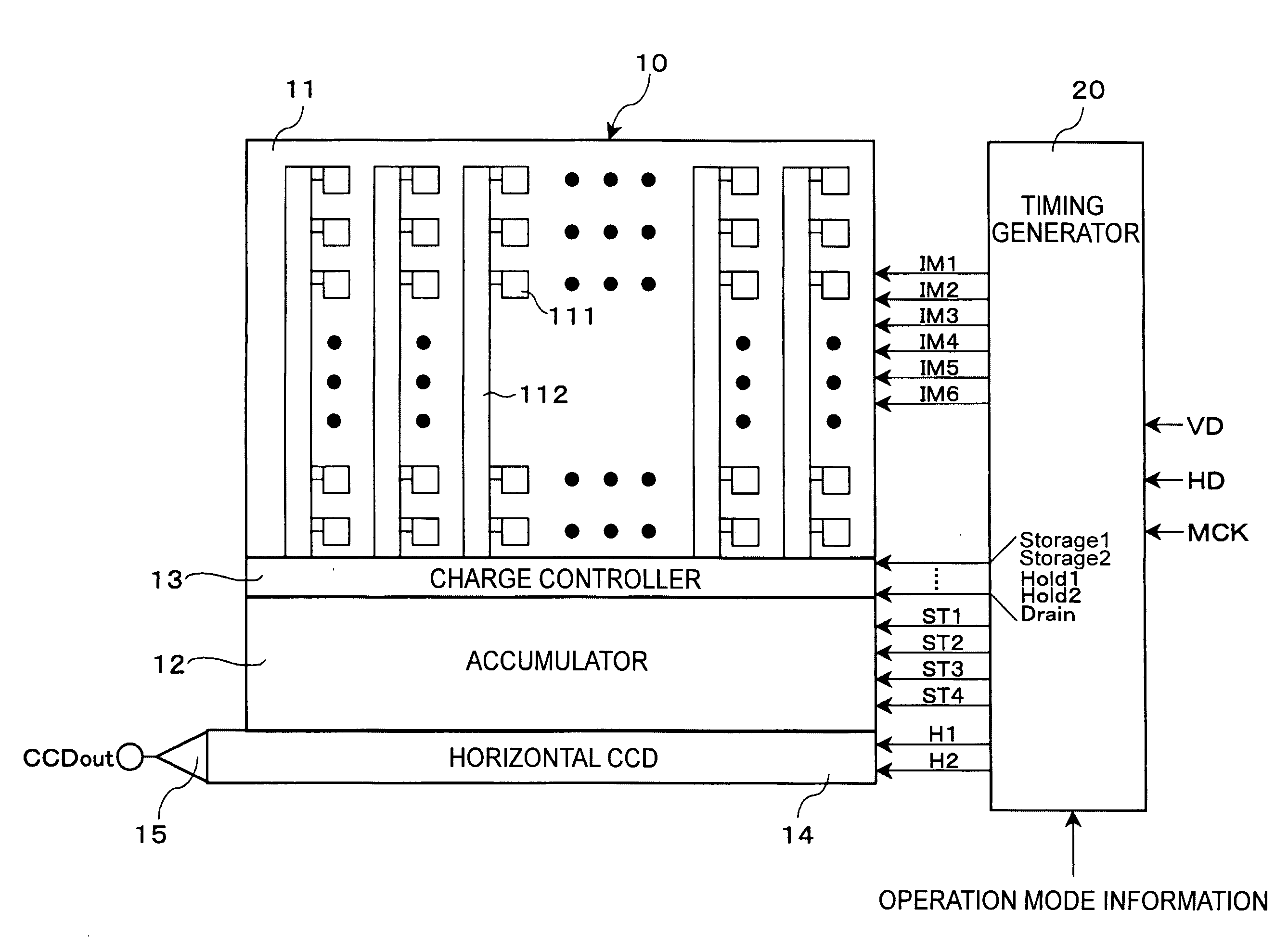
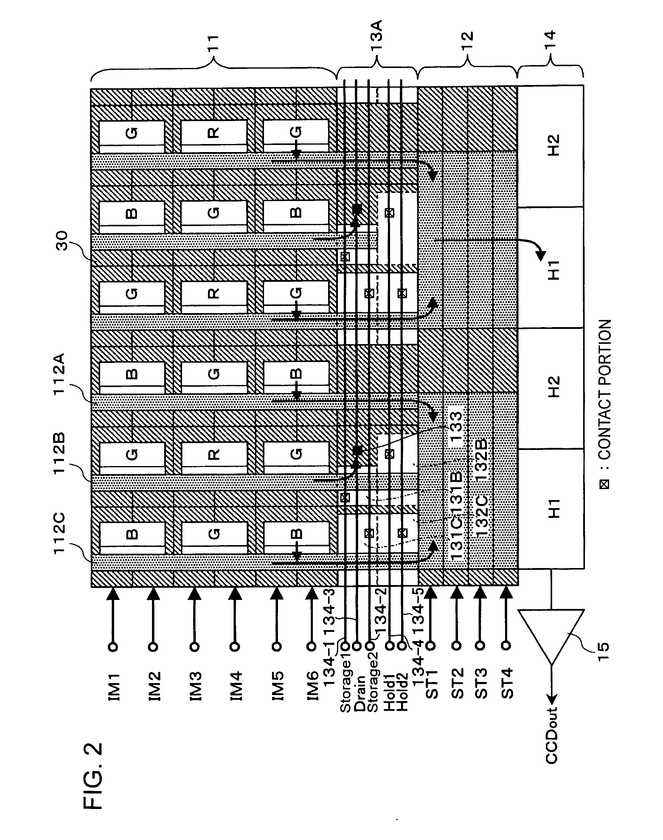
[0043]FIG. 2 is a schematic plan pattern view showing the configuration of the main part including a charge controller 13A according to a first embodiment of the present invention. Color coding of a color filter (not shown) provided on the top layer of the imaging unit 11 is based on two (horizontal) by two (vertical) pixel patterns, by way of example, and the charge controller 13A performs processing in units of three columns (i.e., three horizontal pixels).

[0044] In a predetermined operation mode, in units of a plurality of columns of the plurality of vertical CCDs 112, and the charge controller 13A according to the first embodiment stops transferring charges from a vertical CCD 112 in a predetermined column of the plurality of columns to thin out the charges, and adds signal charges transferred from the two or more remaining vertical CCDs 112 to output the added signal charges. This processing is hereinafter referred to as horizontal thinning-out and addition processing. In anot...

second embodiment

[0095]FIG. 7 is a schematic plan pattern view showing the configuration of the main part including a charge controller 13B according to a second embodiment of the present invention. In FIG. 7, the portions equivalent to those shown in FIG. 2 are identified by the same reference numerals. Color coding of a color filter (not shown) provided on the top layer of the imaging unit 11 is based on two (horizontal) by two (vertical) pixel patterns, by way of example, and the charge controller 13B performs processing in units of four columns (i.e., four horizontal pixels).

[0096] In a predetermined operation mode, a plurality of columns of the vertical CCDs 112 are used as a unit, and the charge controller 13B according to the second embodiment stops transferring charges from a vertical CCD 112 in a predetermined column of the plurality of columns to thin out the charges, and reads out the signal charges transferred from the remaining vertical CCDs 112 to the accumulator 12. This processing i...

application examples

[0131] The FIT-type CCD imaging device 10 including the above-described charge controller 13A or 13B according to the first or second embodiment is suitable to mount as an imaging device in an imaging apparatus (camera module), particularly, a consumer imaging apparatus, e.g., a digital still camera.

[0132]FIG. 11 is a block diagram of an imaging apparatus (e.g., a digital still camera) according to an embodiment of the present invention in which the FIT-type CCD imaging device 10 including the charge controller 13A or 13B according to the first or second embodiment is mounted as an imaging device.

[0133] Referring to FIG. 11, the imaging apparatus according to the present embodiment includes an imaging device 31, a driving circuit 32 that drives the imaging device 31, a lens 33 that focuses incident light (image light) from an object (not shown) onto an imaging surface of the imaging device 31, a signal processing circuit 34 that processes an output signal of the imaging device 31,...


PUM


Abstract

A solid-state imaging device includes an imaging unit, a charge control unit, and a horizontal transfer unit. The imaging unit includes a plurality of pixels arranged into a matrix for performing photoelectric conversion, and a plurality of vertical transfer units arranged in columns for vertically transferring signal charges of the plurality of pixels on a column-by-column basis. In a predetermined operation mode, a predetermined number of columns greater than one are used as a unit, and the charge control unit stops transferring charges from a vertical transfer unit in a predetermined column of the predetermined number of columns, and adds the signal charges transferred from the vertical transfer units in the two or more remaining columns of the predetermined number of columns to output the added signal charges. The horizontal transfer unit horizontally transfers the signal charges output from the charge control unit.

Description

CROSS REFERENCES TO RELATED APPLICATIONS [0001] The present invention contains subject matter related to Japanese Patent Application JP 2004-315490 filed in the Japanese Patent Office on Oct. 29, 2004, the entire contents of which are incorporated herein by reference. BACKGROUND OF THE INVENTION [0002] 1. Field of the Invention [0003] The present invention relates to solid-state imaging devices, methods for driving solid-state imaging devices, and imaging apparatuses. More specifically, the present invention relates to a charge-transfer solid-state imaging device, such as a charge-coupled-device (CCD) imaging device, a method for driving the solid-state imaging device, and an imaging apparatus, such as a digital still camera, including the charge-transfer solid-state imaging device as an imaging device. [0004] 2. Description of the Related Art [0005] Imaging apparatuses, e.g., digital still cameras (DSCs), include all-pixel-readout solid-state imaging devices, such as CCD imaging de...

Claims


Application Information

Patent Timeline
IPC IPC(8): H04N5/335H01L27/148H04N5/345H04N5/347H04N5/359H04N5/372H04N5/376H04N5/378
CPCH04N3/1562H04N5/343H04N5/3456H04N5/3458H04N5/347H04N5/3722H04N25/42H04N25/445H04N25/46H04N25/715H04N25/447H04N25/62H04N25/75
Inventor HIROTA, ISAO
Owner SONY CORP
Why Eureka
Try Eureka