Switching element, line-switching device and logic circuit

a technology of logic circuit and switching element, which is applied in the direction of semiconductor devices, digital storage, instruments, etc., can solve the problems of large leakage current of sram incorporated in each crossbar circuit, increasing the power consumption of the entire circuit,

Inactive Publication Date: 2006-05-18
KK TOSHIBA
View PDF3 Cites 45 Cited by
  • Summary
  • Abstract
  • Description
  • Claims
  • Application Information

AI Technical Summary

Benefits of technology

[0050]FIG. 17A is a circuit diagram useful in explaining the advantages of the eleventh embodiment, and illustrating a case where a two-terminal solid electrolyte switch is used as a memory element;
[0051]FIG. 17B is a circuit diagram useful in explaining the advantages of the eleventh embodiment, and illustrating a case where a four-terminal solid electrolyte switch is used as a memory element;

Problems solved by technology

However, this type of device has the following problem.
Further, the leakage current of the SRAM incorporated in each crossbar circuit is large.
In a microfabrication technique of 0.1 μm or less, the leakage current of the transistors is significantly increased in accordance with the development of microfabrication, thereby increasing the power consumption of the entire circuit.

Method used


Image

  • Switching element, line-switching device and logic circuit
  • Switching element, line-switching device and logic circuit
  • Switching element, line-switching device and logic circuit

Examples


first embodiment

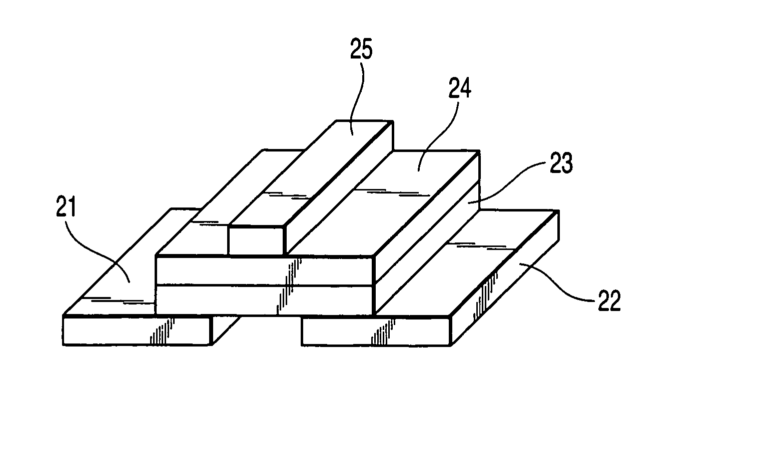
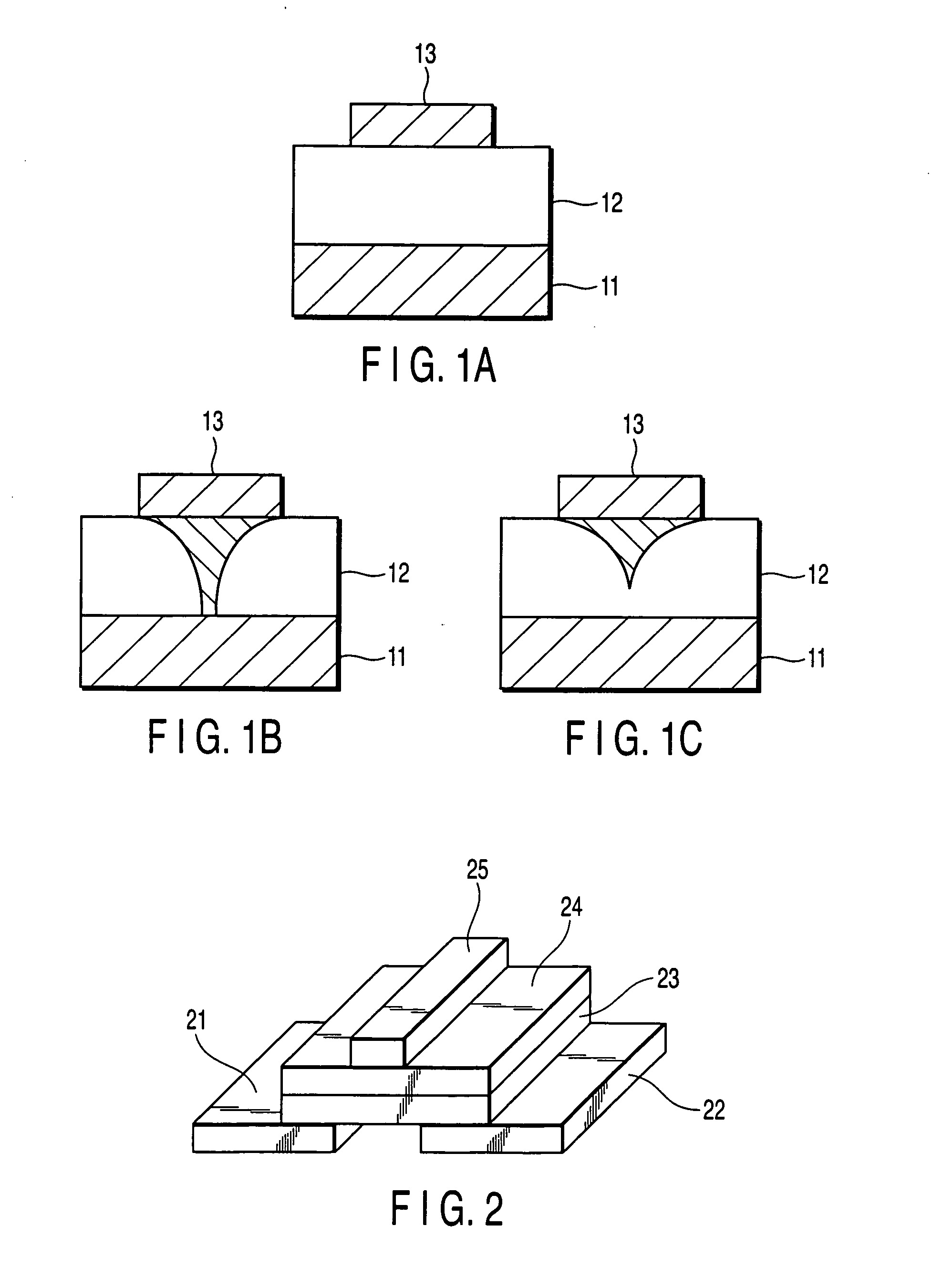
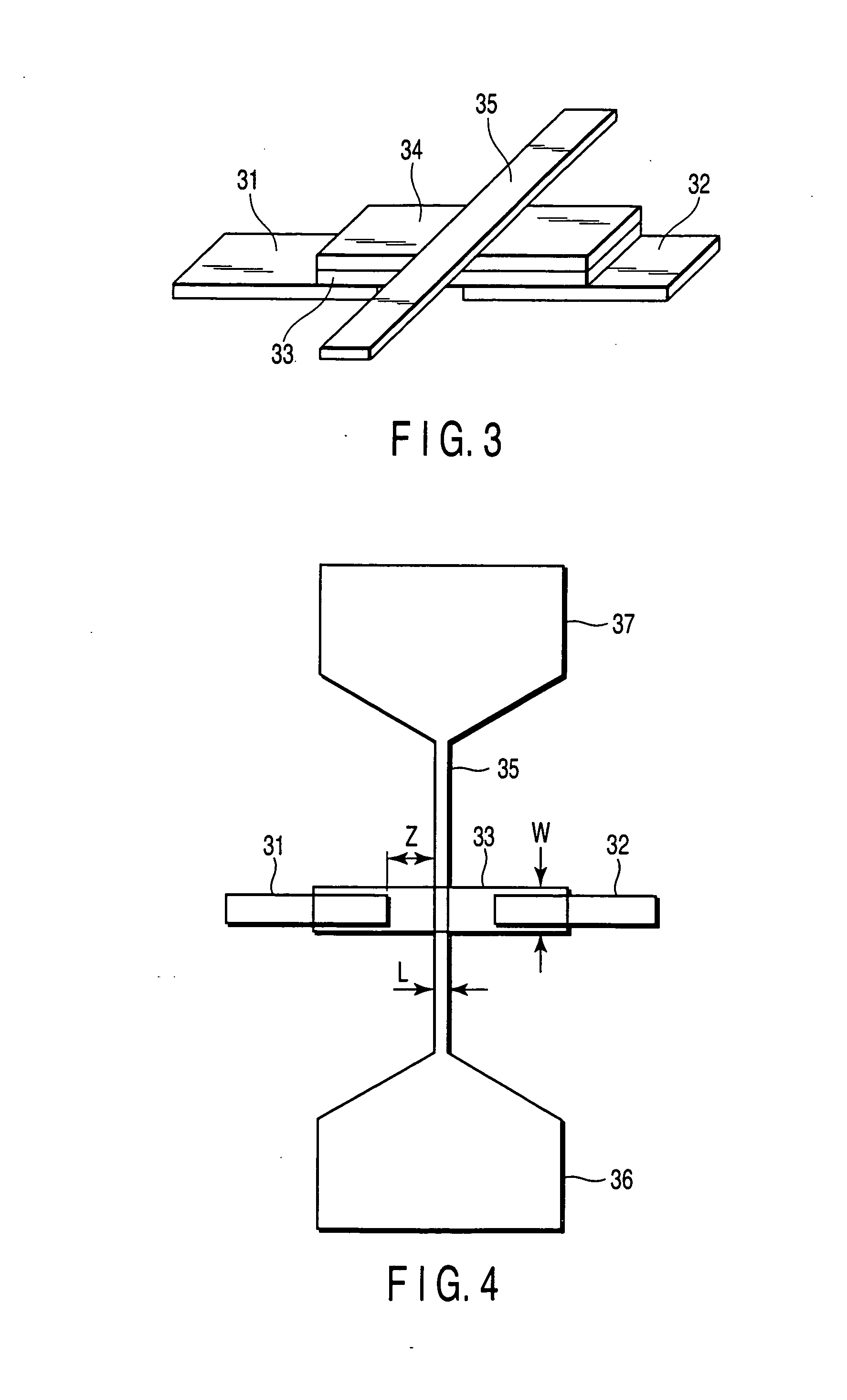
[0065]FIGS. 3 and 4 are schematic views showing the structure of a switching element according to a first embodiment of the invention. FIG. 3 is a perspective view, and FIG. 4 is a plan pattern diagram. In the figures, reference numeral 31 denotes an input electrode, reference numeral 32 denotes an output electrode, and reference numeral 33 denotes a phase change film. Further, reference numeral 34 denotes an insulation film, reference numeral 35 denotes a resistance heating member, and reference numerals 36 and 37 denote conducting electrodes.

[0066] The electrodes 31 and 32 are located on a substrate, not shown, with a certain distance therebetween, and the phase change film 33 bridges the electrodes 31 and 32. More specifically, the phase change film 33 continuously grows from the upper surface of the input electrode 31 to that of the output electrode 32. The phase change film 33 is formed of, for example, GeSeTe, and has its resistance varied in accordance with the state of the ...

second embodiment

[0079]FIG. 6 is a circuit diagram illustrating a line-switching device according to a second embodiment of the invention. This device is part of an FPGA.

[0080] On a substrate, not shown, a plurality of logic circuits 63 are provided, a plurality of lines (first lines) 61 are arranged in the row direction, and a plurality of lines (second lines) 62 are arranged in the column direction. The terminal of each logic circuit 63 is connected to the corresponding one of the lines 61.

[0081] A switching element 64 is provided as a crossbar circuit at each intersection of the lines 61 and 62. One electrode of the switching element 64 is connected to the line 61, and the other electrode is connected to the line 62. The ON / OFF of the switching element 64 is controlled by a control command from a control circuit 65.

[0082] The switching element 64 employed in the second embodiment is similar to that in the first embodiment, and constructed as shown in FIGS. 3 and 4. The conducting electrodes 36...

third embodiment

[0085]FIG. 7 is a plan view schematically illustrating the structure of a switching element according to a third embodiment. In FIG. 7, elements similar to those of FIG. 4 are denoted by corresponding reference numerals, and no detailed description will given thereof.

[0086] The third embodiment differs from the first embodiment in that in the former, a non-linear resistance element 38 is connected in series to the resistance heating member 35. As shown in FIG. 8, in the non-linear resistance element 38, its resistance (and hence the amount of the current flowing therethrough) is varied when the polarity of the voltage is varied, even if the voltage level is not varied.

[0087] When the non-linear resistance element 38 is connected in series to the resistance heating member 35, even if the absolute value of the voltage applied between the conducting electrodes 36 and 37 is unchanged, the amount of the current flowing therethrough can be varied simply by varying the application direct...


PUM


Abstract

A switching element for ON/OFF switching includes a pair of electrodes provided on a substrate separately from each other, a phase change film contacting the electrodes and having its resistance varied in accordance with the history of heating, and a heating mechanism for heating the phase change film.

Description

CROSS-REFERENCE TO RELATED APPLICATIONS [0001] This application is based upon and claims the benefit of priority from prior Japanese Patent Applications No. 2004-333254, filed Nov. 17, 2004; and No. 2005-092288, filed Mar. 28, 2005, the entire contents of both of which are incorporated herein by reference. BACKGROUND OF THE INVENTION [0002] 1. Field of the Invention [0003] The present invention relates to a switching element using a phase change film having its resistance varied in accordance with the state of crystal. It also relates to a line-switching device and logic circuit using the switching element. [0004] 2. Description of the Related Art [0005] Conventional crossbar circuits used for a field programmable gate array (FPGA) comprise an SRAM formed of six transistors, and a MOSFET as a switching element (see T. Sakamoto, et al., Technical Digest of International Solid State Circuit Conference 2004, No. 1603). When “0” is written to the SRAM, the MOSFET is turned on, while whe...

Claims


Application Information

Patent Timeline
Patent Type & Authority Applications(United States)
IPC IPC(8): H01L29/74
CPCG11C13/0004G11C13/0069G11C2013/008H01L27/2409H01L45/06H01L45/085H01L45/1206H01L45/1213H01L45/1226H01L45/1266H01L45/1286H01L45/142H01L45/143H01L45/144H01L45/1608H01L45/1625H01L45/1675H10N70/253H10N70/257H10N70/245H10N70/823H10N70/8613H10N70/8822H10N70/231H10N70/8825H10N70/028H10N70/026H10N70/8828H10N70/063H10B63/20H10N70/021H10N70/8416
Inventor FUJITA, SHINOBUABE, KEIKO
Owner KK TOSHIBA
Why Eureka
Try Eureka