

Heater for annealing trapped charge in a semiconductor device
a technology for semiconductor devices and insulators, applied in semiconductor devices, semiconductor/solid-state device details, electrical devices, etc., can solve problems such as electrical devices to malfunction
- Summary
- Abstract
- Description
- Claims
- Application Information
AI Technical Summary
Benefits of technology
Problems solved by technology
Method used
Image

Examples
Embodiment Construction
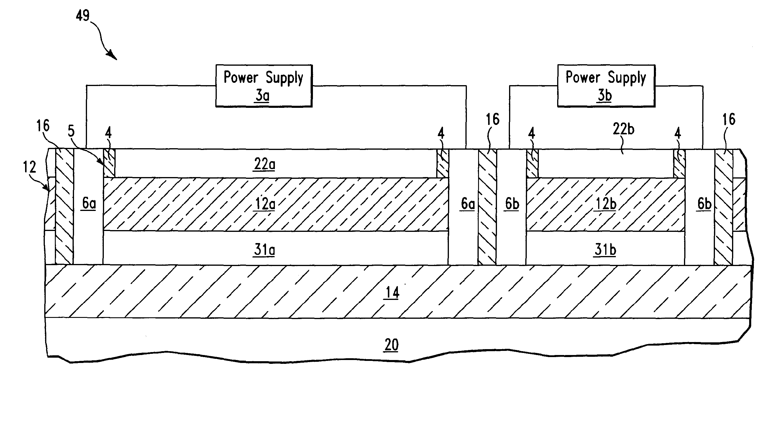
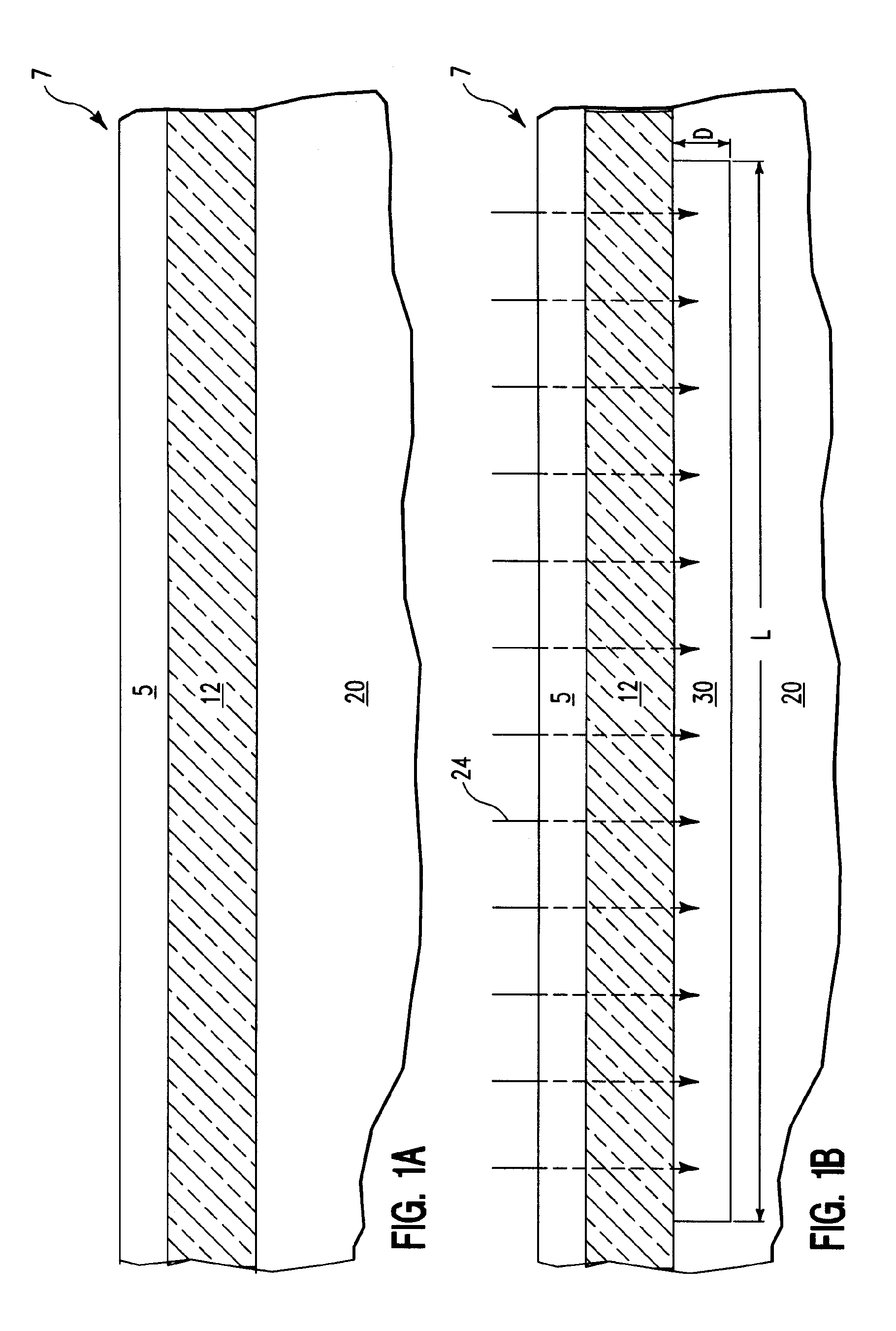
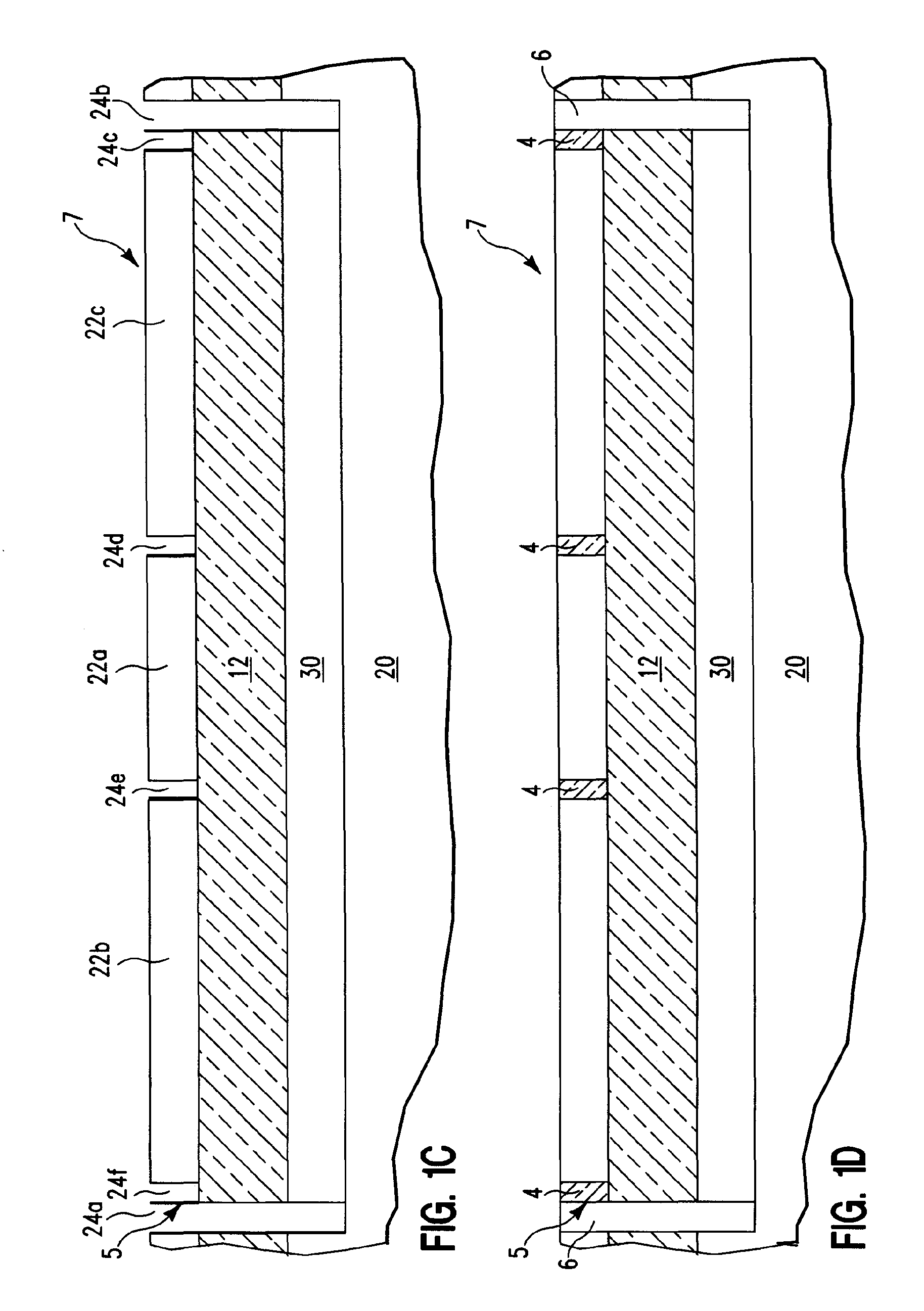
[0017]FIG. 1A-1E illustrate a cross sectional view of a forming method and structure for forming a semiconductor structure 2 comprising a heating element 30, in accordance with embodiments of the present invention. The forming method and structure for forming the semiconductor structure 2 of FIG. 1A-1E also applies to the formation of semiconductor structures 32, 40, and 49 of FIGS. 2, 3, and 4.
[0018]FIG. 1A illustrates a semiconductor substrate 7 processed to be a silicon on insulator (SOI) semiconductor structure 2, in accordance with embodiments of the present invention. The semiconductor substrate 7 may comprise silicon. The semiconductor substrate 7 comprises a bulk layer 20, an insulator layer 12, and a device layer 5. The semiconductor substrate 7 comprising the bulk layer, the insulator layer 12, and the device layer 5 may be formed by any method known to a person of ordinary skill in the art such as, inter alia, SIMOX, smart cut, deep oxygen implant, etc. The term “bulk la...
PUM
 Abstract
Description
Claims
Application Information