Integrated circuit component and mounting method thereof

a technology of integrated circuits and components, applied in the direction of cross-talk/noise/interference reduction, sustainable manufacturing/processing, final product manufacturing, etc., can solve the problems of manufacturing process technical/cost problems, easy generation of switching noise, etc., to achieve effective reduction of switching noise from an integrated circuit, low cost, and easy mounting

Inactive Publication Date: 2006-05-25
FUJITSU LTD
View PDF3 Cites 18 Cited by
  • Summary
  • Abstract
  • Description
  • Claims
  • Application Information

AI Technical Summary

Benefits of technology

[0026] In view of the foregoing, it is an object of the present invention to provide an integrated circuit component capable of easily mounting at low cost a chip part which adjusts impedance of wiring patterns as well as capable of effectively reducing switching noise from an integrated circuit. It is another object of the present invention to provide a method for mounting the chip part.

Problems solved by technology

However, since response speed of the power itself cannot follow current fluctuation of the LSI and the response speed is delayed due to inductance components in a feeder line of the power, switching noise is generated.
As a result, there is a problem that the above-described switching noise is easily generated due to the lengths of the wiring patterns 121 and 141.
However, the technology described in Japanese Unexamined Patent Publication No. 2001-102512 (FIG. 1) has the following problems.
Thus, the manufacturing process has a technical / cost problem.
That is, a scope of design is limited by designers and manufacturers.
Accordingly, a mounting position, number and characteristics of a bypass capacitor or a damping resistor must be previously determined at the time of order placement and therefore, are difficult to be changed later.
Particularly in the damping resistor, a problem may occur in a characteristic assessment after the manufacture of the first lot due to shortage of characteristic investigation in designing of a wiring board or due to variation in characteristics of LSI.
As a result, any action may not be easily taken due to problems such as a period or cost.
Therefore, the response speed of the power is delayed due to inductance components in the transmission path of the power, and as a result, an effect of reducing switching noise cannot be greatly obtained.

Method used


Image

  • Integrated circuit component and mounting method thereof
  • Integrated circuit component and mounting method thereof
  • Integrated circuit component and mounting method thereof

Examples


first embodiment

[0051] A first embodiment of the present invention will be described.

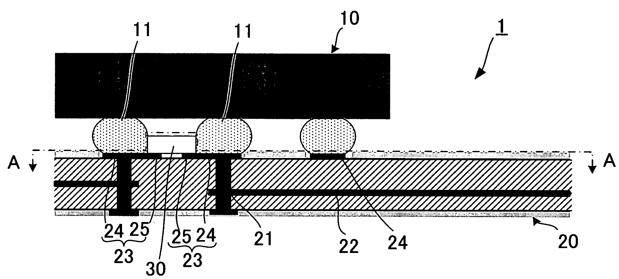
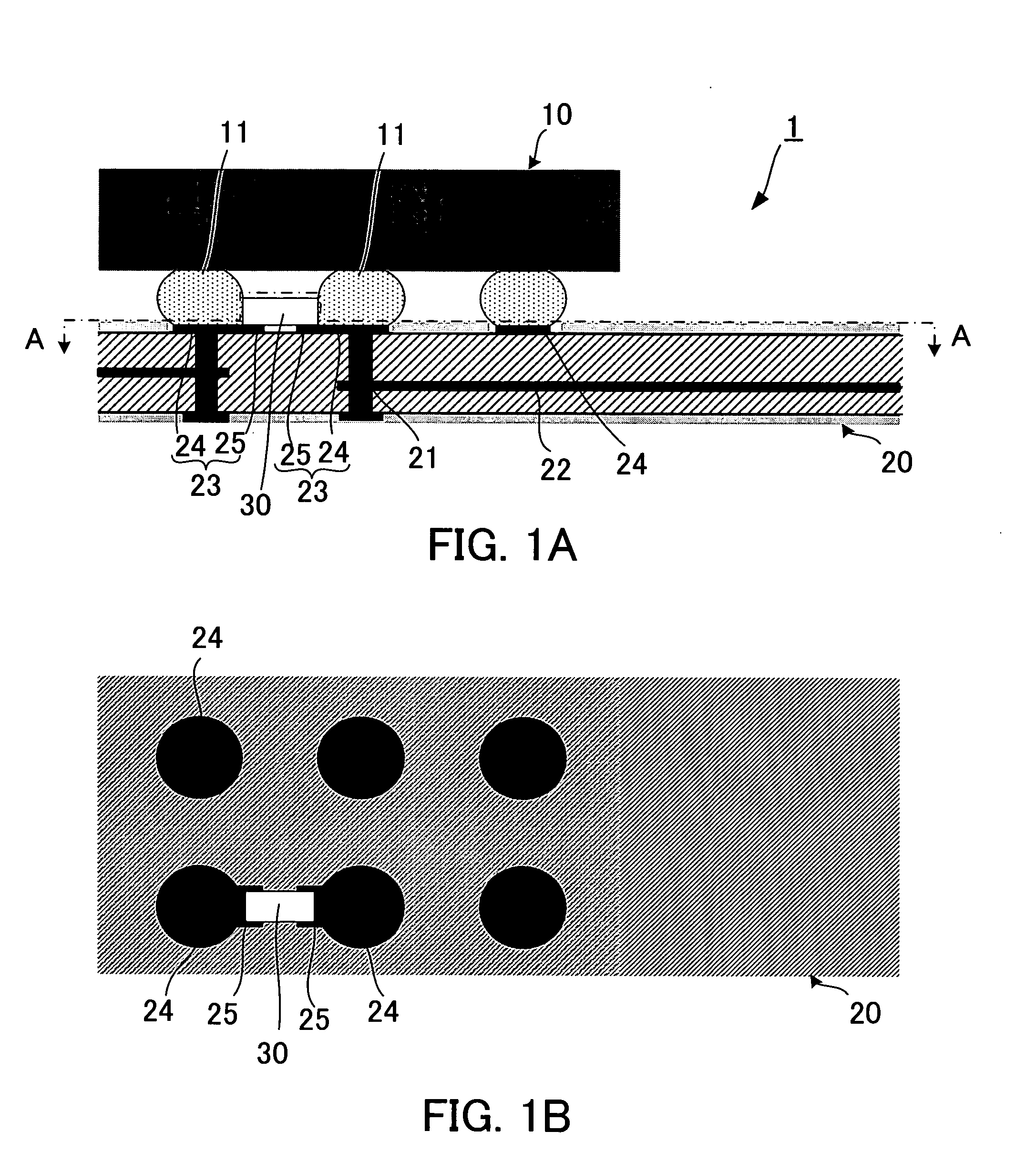
[0052] The present embodiment relates to an integrated circuit component constituted by mounting a BGA-type LSI chip and a bypass capacitor on a wiring board. FIG. 1 illustrates a mounting structure of the integrated circuit component. FIG. 1A is a sectional view of FIG. 1. FIG. 1B is a sectional view taken along a line A-A of FIG. 1.

[0053] As shown in FIG. 1A, an integrated circuit component 1 is composed of a BGA-type LSI chip 10 (an integrated circuit module) and a wiring board 20 for mounting the LSI chip 10 through solder bumps 11 (metal bumps).

[0054] In the LSI chip 10, a plurality of the solder bumps 11 are formed in a line on a surface of the LSI chip 10 to be mounted on a wiring board 20. These solder bumps 11 constitutes an external terminal of the chip 10. A mounting method of the solder bumps 11 in a manufacturing process of the LSI chip 10 is performed by reflow through the solder paste in the same ...

second embodiment

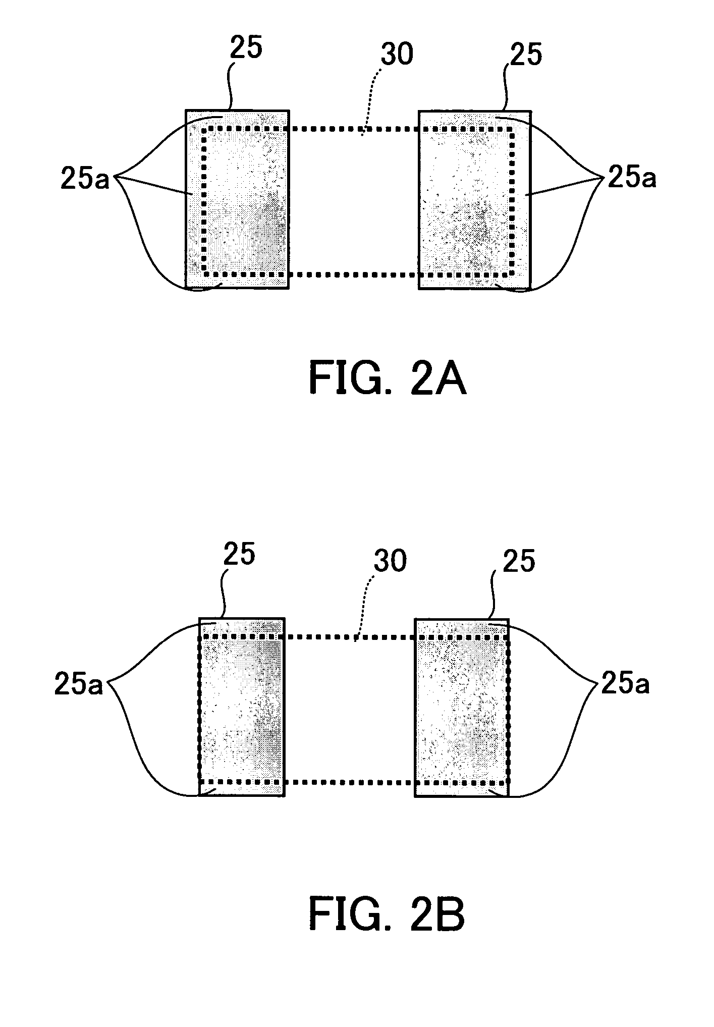
[0073] Next, a second embodiment of the present invention will be described. The present embodiment has the same constitution as in the first embodiment except for being different from the first embodiment in the mounting mode of the chip part. Therefore, in the figure, the same elements as those of the first embodiment are indicated by the same reference numerals as in the first embodiment, if necessary, and the description is omitted. FIG. 8 illustrates a mounting surface of the chip part of the present embodiment.

[0074] As shown in FIG. 8A, in the integrated circuit component of the present embodiment, the bypass capacitor 30 (the chip part) is mounted in a position at a distance from an axis line L (a dashed line in the figure) along an adjacent direction of the adjacent solder bumps 11 (a broken line in the figure).

[0075] Specifically, the integrated circuit component of the present embodiment is applicable to the following case. That is, depending on a size of the solder bum...

third embodiment

[0086] Next, a third embodiment of the present invention will be described. The present embodiment has the same constitution as in the first embodiment except for being different from the first embodiment in the mounting mode of the chip part. Therefore, in the figure, the same elements as those of the first embodiment are indicated by the same reference numerals as in the first embodiment, if necessary, and the description is omitted. FIG. 11 illustrates a mounting surface of the chip part of the present embodiment.

[0087] As shown in FIG. 11A, also in the integrated circuit component of the present embodiment, the bypass capacitor 30 (the chip part) is mounted in a position at a distance from an axis line L (a dashed line in the figure) along an adjacent direction of the adjacent solder bumps 11 (a broken line in the figure) in the same manner as in the second embodiment.

[0088] Specifically, on a surface of the wiring board 20, the footprints 25 and 25 for mounting the bypass cap...


PUM


Abstract

Disclosed are an integrated circuit component capable of simply mounting at low cost a chip part which adjusts impedance of wiring patterns as well as capable of effectively reducing switching noise from an integrated circuit, and a method for mounting the chip part. The integrated circuit component of the present invention has a constitution that a bypass capacitor is mounted on a wiring board side of a gap between the wiring board and an LSI chip. Therefore, as compared with a case where the capacitor is mounted on the LSI chip side, a transmission path through the capacitor can be extremely shortened. As a result, inductance components of the feeder line can be reduced, so that a response delay of power transmitted through the feeder line can be sufficiently suppressed.

Description

CROSS-REFERENCE TO RELATED APPLICATIONS [0001] This application is a continuing application, filed under 35 U.S.C. §111(a), of International Application PCT / JP2003 / 011173, filed Sep. 1, 2003.BACKGROUND OF THE INVENTION [0002] 1. Field of the Invention [0003] The present invention relates to an integrated circuit component constituted by mounting, on a wiring board having mounted thereon an integrated circuit module, a chip part which adjusts impedance of wiring patterns. The present invention also pertains to a method for mounting the chip part. [0004] 2. Description of the Related Art [0005] As this type of integrated circuit component, there is conventionally known, for example, a component having a bypass capacitor as a chip part as shown in FIG. 15 or a component having a damping resistor as a chip part as shown in FIG. 16. [0006] First, an integrated circuit component as shown in FIG. 15 is described. FIG. 15A is a sectional view of an integrated circuit component having a bypa...

Claims


Application Information

Patent Timeline
Patent Type & Authority Applications(United States)
IPC IPC(8): H01L27/10H01L21/60H01L23/12H01L23/50H01L23/66H01L25/00H05K1/02H05K1/11H05K3/34
CPCH01L23/49838H01L2224/16235H01L23/66H01L24/81H01L2224/16H01L2224/81193H01L2224/8121H01L2224/81815H01L2924/01082H01L2924/14H01L2924/19041H01L2924/19043H01L2924/19103H01L2924/30105H01L2924/30107H01L2924/3011H05K1/023H05K1/0231H05K1/025H05K1/111H05K3/3436H05K3/3442H05K2201/10022H05K2201/10515H05K2201/10636H05K2201/10734H01L2924/01005H01L2924/01006H01L2924/01033H01L2924/01074H01L2924/014H01L2224/16225H01L23/50H01L2224/16105H01L2224/16265H01L2224/16106H01L24/16H01L24/17H01L2224/17104Y02P70/50H01L2924/00012
Inventor TESHIMA, YASUHIRONAKAMA, NOBORU
Owner FUJITSU LTD
Why Eureka
Try Eureka