Ferroelectric integrated circuit devices having an oxygen penetration path and methods for manufacturing the same

a ferroelectric integrated circuit and oxygen penetration technology, applied in semiconductor devices, capacitors, electrical devices, etc., can solve the problems of device performance degradation after the backend integration process, write operation speed ranging from several tens of nanoseconds to several hundred of nanoseconds, etc., to reduce oxygen vacancies in the ferroelectric layer

Inactive Publication Date: 2006-05-25
SAMSUNG ELECTRONICS CO LTD
View PDF13 Cites 8 Cited by
  • Summary
  • Abstract
  • Description
  • Claims
  • Application Information

AI Technical Summary

Benefits of technology

[0013] In further embodiments of the present invention, forming a common via hole is followed by recovery annealing the integrated circuit device to reduce oxygen vacancies in the ferroelectric layer by providing oxygen to the ferroelectric layer through the oxygen penetration path. Following forming of the encapsulated barrier layer and before forming of the common via hole, the the integrated circuit device may be exposed to hydrogen gas during a backend process. Forming the common via hole may include forming a slit-type common via hole exposing at least part of the at least one plate line and recovery annealing may be followed by forming a common plate line in the common via hole that electrically contacts the at least one plate line.

Problems solved by technology

In addition, with optimized designs, ferroelectric memory devices may result in write operation speeds ranging from several hundreds of nanoseconds to several tens of nanoseconds.
As a result, device performance after the backend integration process may be degraded.

Method used


Image

  • Ferroelectric integrated circuit devices having an oxygen penetration path and methods for manufacturing the same
  • Ferroelectric integrated circuit devices having an oxygen penetration path and methods for manufacturing the same
  • Ferroelectric integrated circuit devices having an oxygen penetration path and methods for manufacturing the same

Examples


Embodiment Construction

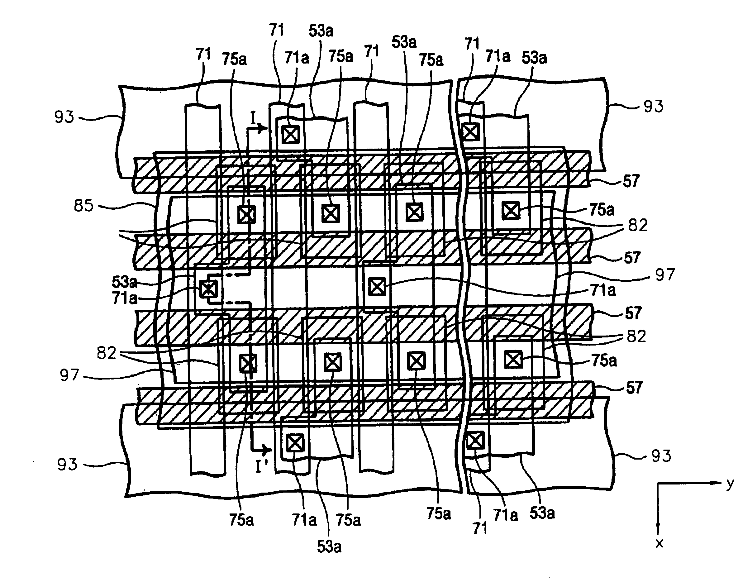
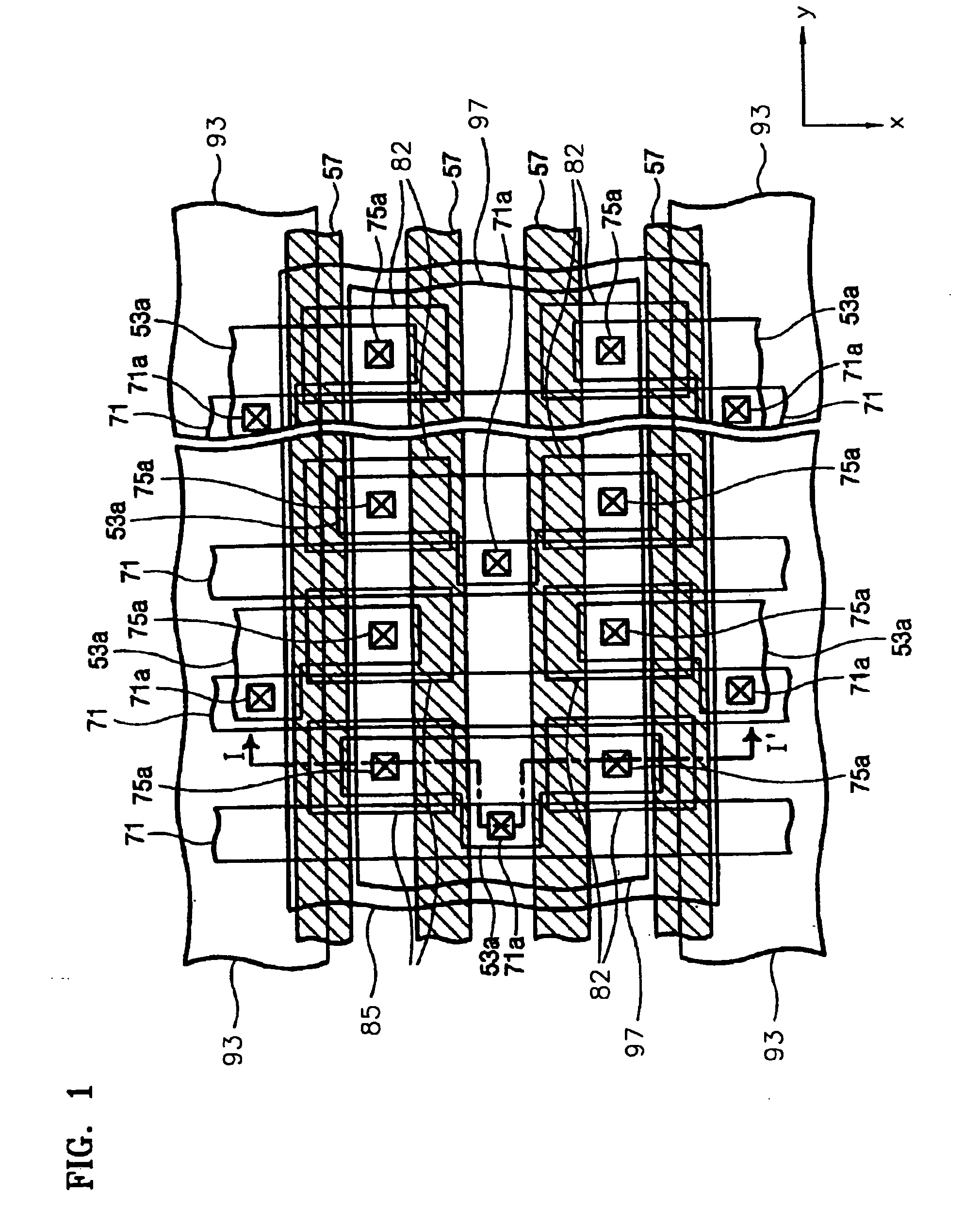
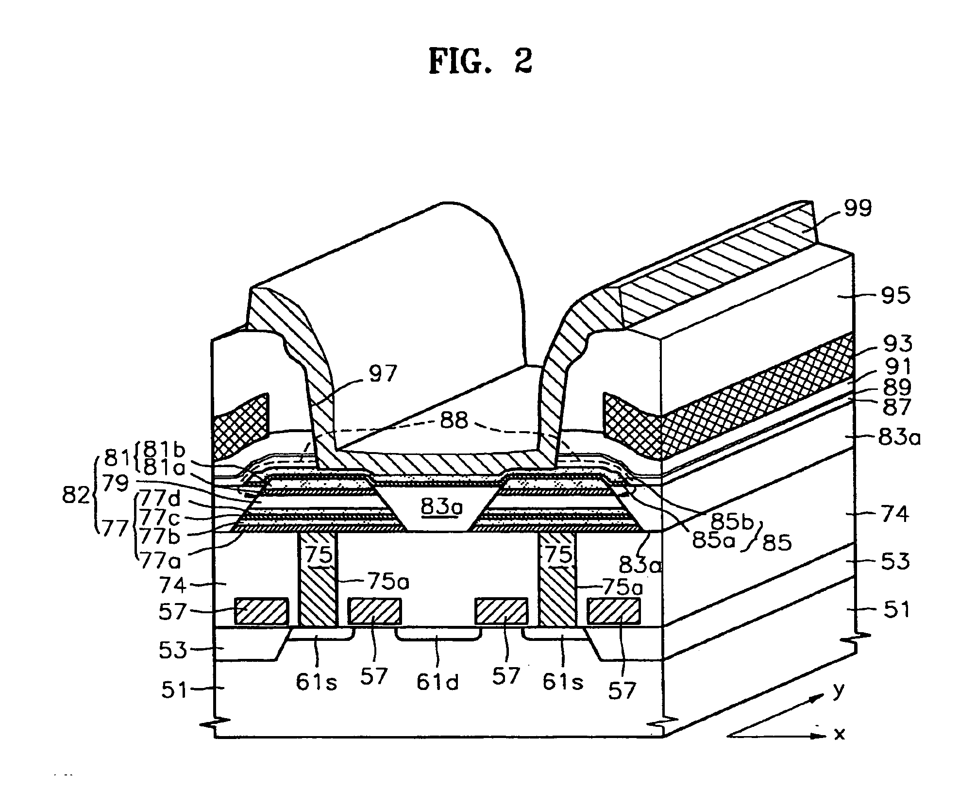
[0034] The present invention now will be described more fully hereinafter with reference to the accompanying drawings, in which typical embodiments of the invention are shown. This invention may, however, be embodied in many different forms and should not be construed as limited to the embodiments set forth herein. Rather, these embodiments are provided so that this disclosure will be thorough and complete, and will fully convey the scope of the invention to those skilled in the art. In the drawings, the relative sizes of regions may be exaggerated for clarity. It will be understood that when an element such as a layer, region or substrate is referred to as being “on” another element, it can be directly on the other element or intervening elements may also be present. In contrast, when an element is referred to as being “directly on” another element, there are no intervening elements present. Moreover, each embodiment described and illustrated herein includes its complementary condu...


PUM


Abstract

Ferroelectric integrated circuit devices, such as memory devices, are formed on an integrated circuit substrate. Ferroelectric capacitor(s) are on the integrated circuit substrate and a further structure on the integrated circuit substrate overlies at least a part of the ferroelectric capacitor(s). The further structure includes at least one layer providing a barrier to oxygen flow to the ferroelectric capacitor(s). An oxygen penetration path contacting the ferroelectric capacitor(s) is interposed between the ferroelectric capacitor(s) and the further structure. The layer providing a barrier to oxygen flow may be an encapsulated barrier layer. Methods for forming ferroelectric integrated circuit devices, such as memory devices, are also provided.

Description

RELATED APPLICATION [0001] This application claims priority from Korean Application No. 2002-5421, filed Jan. 30, 2002, the disclosure of which is hereby incorporated herein by reference. BACKGROUND OF THE INVENTION [0002] The present invention relates to integrated circuit devices and, more particularly, to ferroelectric integrated circuit devices, such as memory devices, including a ferroelectric capacitor and methods for manufacturing the same. [0003] Recently, ferroelectric memory devices using ferroelectric layers have been considered as an alternative approach for certain memory applications. Ferroelectric memory devices are generally divided into two categories. The first category includes devices using a ferroelectric capacitor as described, for example, in U.S. Pat. No. 5,523,964. The second category includes devices having a ferroelectric field emission transistor (FET) as described, for example, in U.S. Pat. No. 5,198,994. Ferroelectric memory devices generally use polari...

Claims


Application Information

Patent Timeline
Patent Type & Authority Applications(United States)
IPC IPC(8): H01L29/94H01L21/00H01L27/105H01L21/02H01L21/8246H01L27/115
CPCH01L27/11502H01L27/11507H01L28/55H01L28/57H10B53/30H10B53/00H01L27/105
Inventor JOO, HEUNG-JINKIM, KI-NAMSONG, YOON-JONG
Owner SAMSUNG ELECTRONICS CO LTD
Why Eureka
Try Eureka