Semiconductor device, method for manufacturing semiconductor device, and method for forming oxide film

a semiconductor film and semiconductor technology, applied in the direction of semiconductor devices, electrical devices, transistors, etc., can solve the problems of difficult to reduce the oxygen vacancies in the oxide semiconductor film, poor electric characteristics of the transistor, etc., and achieve high on-state current, high carrier mobility, and increased carrier mobility

Active Publication Date: 2017-01-19
SEMICON ENERGY LAB CO LTD
View PDF6 Cites 2 Cited by
  • Summary
  • Abstract
  • Description
  • Claims
  • Application Information

AI Technical Summary

Benefits of technology

[0012]In a transistor including an oxide semiconductor, hydrogen (including water, a hydrogen ion, a hydroxide ion, and the like) and oxygen vacancies in the oxide semiconductor film causes the transistor to have poor electric characteristics. For example, the threshold voltage of a transistor which includes an oxide semiconductor film including hydrogen and oxygen vacancies tends to shift in the negative direction, and thus the transistor tends to be normally on. This is because charge is generated owing to the hydrogen and oxygen vacancies in the oxide semiconductor film to reduce the resistance of the oxide semiconductor film. It is difficult to reduce the oxygen vacancies in the oxide semiconductor film. For example, oxygen vacancies are easily formed in an oxide semiconductor film in the step of forming or etching the oxide semiconductor film.
[0013]In a variety of semiconductor devices such as display devices and semiconductor memory devices, improvement of the electric characteristics of a transistor included in the semiconductor device results in improvement of the performance of the semiconductor device. To manufacture a display device with higher definition, for example, it is important to achieve an increase in the field-effect mobility of the transistor, a reduction in the leakage current of the transistor, and the like.
[0014]In view of the above, an object of one embodiment of the present invention is to provide a semiconductor device including an oxide semiconductor film in which oxygen vacancies are reduced and a method for manufacturing the semiconductor device. Another object of one embodiment of the present invention is to provide a high-performance semiconductor device having favorable electric characteristics and a method for manufacturing the semiconductor device.

Problems solved by technology

In a transistor including an oxide semiconductor, hydrogen (including water, a hydrogen ion, a hydroxide ion, and the like) and oxygen vacancies in the oxide semiconductor film causes the transistor to have poor electric characteristics.
It is difficult to reduce the oxygen vacancies in the oxide semiconductor film.

Method used


Image

  • Semiconductor device, method for manufacturing semiconductor device, and method for forming oxide film
  • Semiconductor device, method for manufacturing semiconductor device, and method for forming oxide film
  • Semiconductor device, method for manufacturing semiconductor device, and method for forming oxide film

Examples


embodiment 1

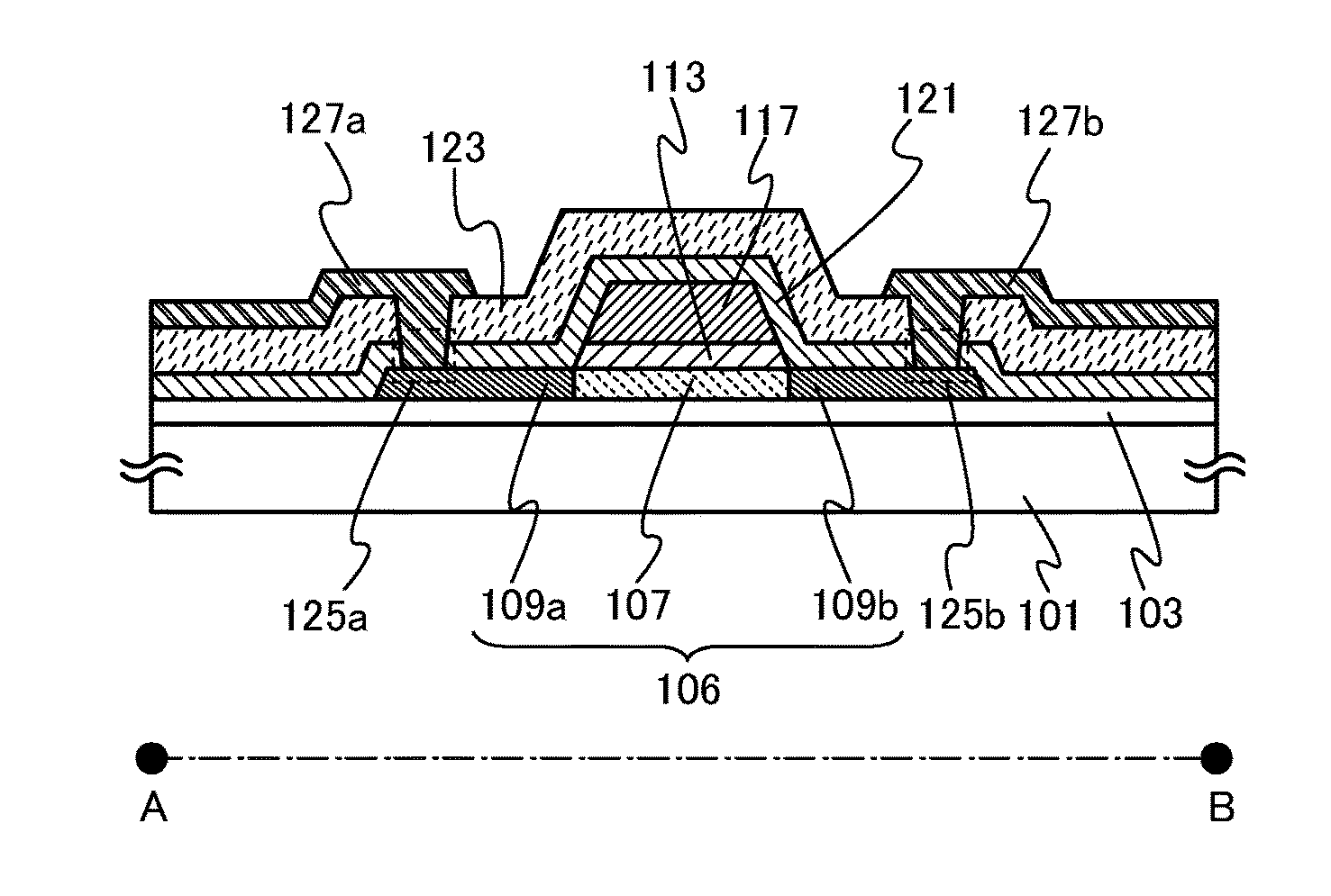
[0066]In this embodiment, a semiconductor device of one embodiment of the present invention will be described with reference to drawings. A transistor will be described as an example of the semiconductor device.

[0067]FIGS. 1A and 1B are a top view and a cross-sectional view which illustrate a transistor 100. FIG. 1A is a top view of the transistor 100, and FIG. 1B is a cross-sectional view taken along dashed-dotted line A-B in FIG. 1A. Note that in FIG. 1A, some components of the transistor 100 (e.g., a substrate 101, a base insulating film 103, and a gate insulating film 113) are omitted for simplicity.

[0068]According to FIGS. 1A and 1B, in the transistor 100, the base insulating film 103 is provided over the substrate 101, an oxide semiconductor film 105 is provided over the base insulating film 103, the gate insulating film 113 is provided over the oxide semiconductor film 105, a gate electrode 117 is provided over the gate insulating film 113, a metal oxide film 121 having an in...

embodiment 2

[0182]In this embodiment, a semiconductor device having a structure which is partly different from that of the semiconductor device described in the above embodiment will be described. Note that a transistor will be described as an example of the semiconductor device also in this embodiment. In this embodiment, the drawings (including reference numerals and hatching patterns) and descriptions in the above embodiment are used as appropriate, and points described in the above embodiment are not repeated in some cases.

[0183]The transistor described in this embodiment has a structure in which the oxide semiconductor film of the transistor described in the above embodiment includes a first region functioning as a channel formation region and a pair of second regions having lower resistance than the first region and functioning as a source region and a drain region. The first region and the pair of second regions can be formed in a self-aligned manner by injection of a dopant with use of ...

embodiment 3

[0210]In this embodiment, a semiconductor device having a structure which is partly different from those of the semiconductor devices described in the above embodiments will be described. Note that a transistor will be described as an example of the semiconductor device also in this embodiment. In this embodiment, the drawings (including reference numerals and hatching patterns) and descriptions in the above embodiments are used as appropriate, and points described in the above embodiments are not repeated in some cases.

[0211]The transistor described in this embodiment has a structure in which the oxide semiconductor film of the transistor described in either of the above embodiments includes a first region, a pair of second regions having lower resistance than the first region, and a pair of third regions having lower resistance than the pair of second regions. The first region, the pair of second regions, and the pair of third regions are formed in a self-aligned manner by injecti...


PUM

PropertyMeasurementUnit
self-bias voltageaaaaaaaaaa
temperatureaaaaaaaaaa

Abstract

One embodiment of the present invention is a semiconductor device at least including an oxide semiconductor film, a gate insulating film in contact with the oxide semiconductor film, and a gate electrode overlapping with the oxide semiconductor film with the gate insulating film therebetween. The oxide semiconductor film has a spin density lower than 9.3×10¹⁶ spins / cm3 and a carrier density lower than 1×10¹⁵ / cm3. The spin density is calculated from a peak of a signal detected at a g value (g) of around 1.93 by electron spin resonance spectroscopy. The oxide semiconductor film is formed by a sputtering method while bias power is supplied to the substrate side and self-bias voltage is controlled, and then subjected to heat treatment.

Description

BACKGROUND OF THE INVENTION[0001]1. Field of the Invention[0002]This document relates to semiconductor devices, method for manufacturing semiconductor devices, and method for forming oxide films.[0003]Note that a semiconductor device in this specification refers to general devices which can function by utilizing semiconductor characteristics; for example, a semiconductor element such as a transistor, a semiconductor circuit including a semiconductor element, an electro-optical device such as a display device, and an electronic device are all semiconductor devices.[0004]2. Description of the Related Art[0005]Transistors used for most flat panel displays typified by a liquid crystal display device and a light-emitting display device are formed using silicon semiconductors such as amorphous silicon, single crystal silicon, and polycrystalline silicon provided over glass substrates. Further, transistors formed using such silicon semiconductors are used in integrated circuits (ICs) and t...

Claims


Application Information

Patent Timeline
Patent Type & Authority Applications(United States)
IPC IPC(8): H01L29/66H01L29/786H01L21/02
CPCH01L29/66969H01L21/02631H01L29/7869H01L29/78621H01L21/02565H01L29/78696H01L29/66742
Inventor NODA, KOSEIHIRAISHI, SUZUNOSUKE
Owner SEMICON ENERGY LAB CO LTD
Why Eureka
Try Eureka