Method for manufacturing semiconductor device

a manufacturing method and semiconductor technology, applied in the direction of transistors, electroluminescent light sources, electric lighting sources, etc., can solve the problems of poor electrical characteristics of transistors, and achieve the effect of improving the electrical characteristics improving the reliability of a semiconductor device using an oxide semiconductor

Active Publication Date: 2016-09-20
SEMICON ENERGY LAB CO LTD
View PDF177 Cites 10 Cited by
  • Summary
  • Abstract
  • Description
  • Claims
  • Application Information

AI Technical Summary

Benefits of technology

[0011]In view of this, an object of one embodiment of the present invention is to improve electrical characteristics of a semiconductor device using an oxide semiconductor. Another object of one embodiment of the present invention is to improve reliability of a semiconductor device using an oxide semiconductor. Another object of one embodiment of the present invention is to reduce oxygen vacancies in an oxide semiconductor. Another object of one embodiment of the present invention is to prevent a transistor from becoming normally-on. Another object of one embodiment of the present invention is to control change, variation, or decrease in the threshold voltage of a transistor. Another object of one embodiment of the present invention is to provide a transistor having low off-state current. Another object of one embodiment of the present invention is to provide a novel semiconductor device or the like.
[0013]One embodiment of the present invention is a transistor including a first oxide semiconductor film, a second oxide semiconductor film, a pair of electrodes in contact with the second oxide semiconductor film, and a third oxide semiconductor film in contact with the second oxide semiconductor film and the pair of electrodes, in which oxygen is added to the first oxide semiconductor film or the third oxide semiconductor film to reduce oxygen vacancies. Further, the oxygen is diffused to the second oxide semiconductor film by heat treatment or the like, so that oxygen vacancies in the second oxide semiconductor film are reduced.
[0016]Note that by adding oxygen to the first oxide semiconductor film and / or the third oxide semiconductor film and then performing heat treatment, oxygen vacancies in the first oxide semiconductor film and / or the third oxide semiconductor film can be reduced.
[0021]With one embodiment of the present invention, electrical characteristics of a semiconductor device using an oxide semiconductor can be improved. With one embodiment of the present invention, reliability of a semiconductor device using an oxide semiconductor can be improved. Furthermore, with one embodiment of the present invention, a novel semiconductor device or the like can be provided. Note that the description of these effects does not disturb the existence of other effects. One embodiment of the present invention does not necessarily have all the effects listed above. Other effects will be apparent from and can be derived from the description of the specification, the drawings, the claims, and the like.

Problems solved by technology

In a transistor using an oxide semiconductor, oxygen vacancies which are one cause of localized states in an oxide semiconductor film lead to poor electrical characteristics of the transistor.

Method used


Image

  • Method for manufacturing semiconductor device
  • Method for manufacturing semiconductor device
  • Method for manufacturing semiconductor device

Examples


embodiment 1

[0076]The threshold voltage of a transistor using an oxide semiconductor film with oxygen vacancies easily shifts in the negative direction, and such a transistor tends to be normally-on. This is because electric charges are generated owing to oxygen vacancies in the oxide semiconductor, and the resistance is reduced. In addition, a transistor using an oxide semiconductor film with oxygen vacancies has such a problem that the electrical characteristics, typically, the threshold voltage, are changed with time or changed by a stress test (typically, a gate bias-temperature (BT) stress test under light irradiation). In this embodiment, a highly reliable semiconductor device in which a change in threshold voltage is small and a manufacturing method thereof will be described. Further, a semiconductor device with excellent electrical characteristics and a manufacturing method thereof will be described.

[0077]In this embodiment, a method for manufacturing a top-gate transistor is described....

embodiment 2

[0285]In this embodiment, a method for reducing oxygen vacancies in an oxide semiconductor film, which is different from the method in Embodiment 1, will be described. This embodiment is different from Embodiment 1 in adding oxygen to an oxide semiconductor film positioned over the pair of electrodes 113a and 113b.

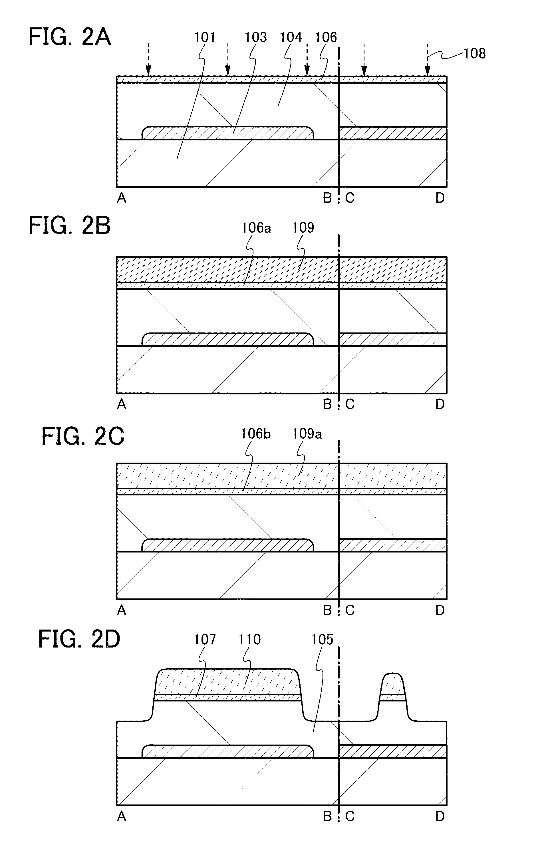
[0286]As illustrated in FIG. 10A, the gate electrode 103 is formed over the substrate 101, and the insulating film 104 is formed over the gate electrode 103. Then, the oxide semiconductor film 106 is formed over the insulating film 104, and the oxide semiconductor film 109 is formed over the oxide semiconductor film 106.

[0287]Next, a mask is formed over the oxide semiconductor film 109 by a lithography process, and part of the insulating film 104, part of the oxide semiconductor film 106, and part of the oxide semiconductor film 109 are etched using the mask; thus, the gate insulating film 105, the oxide semiconductor film 107, and an oxide semiconductor film 110a are for...

embodiment 3

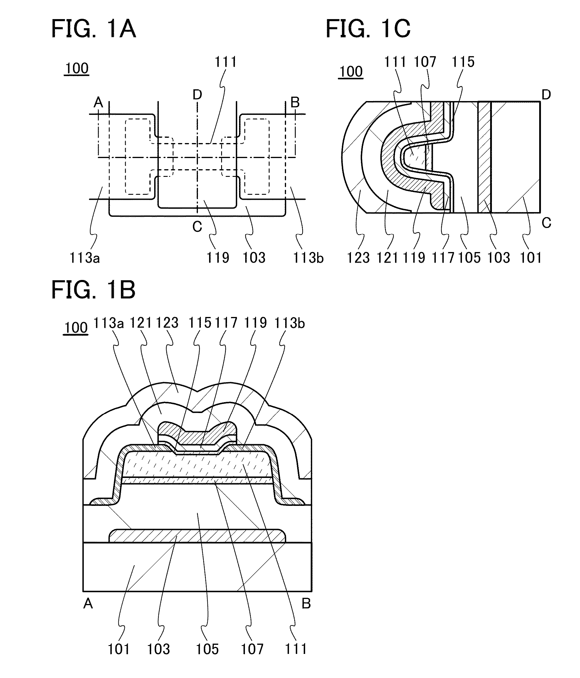
[0309]Transistors each having a stacked structure of oxide semiconductor films different from that of the transistor 100 illustrated in FIGS. 1A to 1C will be described with reference to FIGS. 13A to 13C.

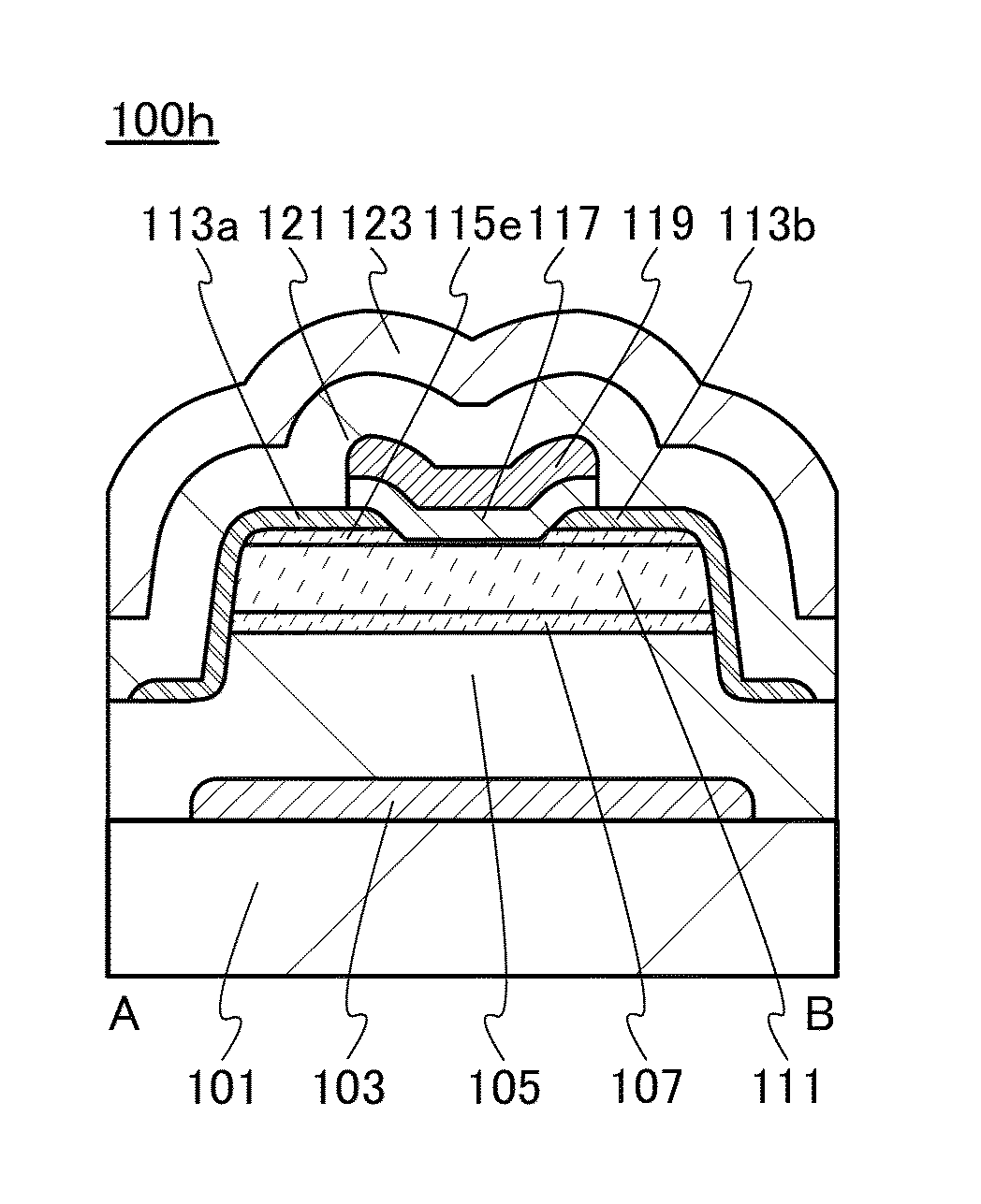
[0310]A transistor 100f illustrated in FIG. 13A is different from the transistor 100 illustrated in FIG. 1B in not including the oxide semiconductor film 115. In other words, the transistor 100f is characterized by including the gate insulating film 117 that is in contact with the oxide semiconductor film 111, the pair of electrodes 113a and 113b, and the gate electrode 119.

[0311]Note that in a method for manufacturing the transistor 100f illustrated in FIG. 13A, the method for forming the oxide semiconductor film 111 described in Embodiment 1 can be used as appropriate.

[0312]A transistor 100g illustrated in FIG. 13B is different from the transistor 100 illustrated in FIG. 1B in not including the oxide semiconductor film 107. In other words, the transistor 100g is characterized by i...


PUM


Abstract

The semiconductor device is manufactured by the following method. A first oxide semiconductor film is formed over a first gate electrode and a first insulating film, oxygen is added to the first oxide semiconductor film, and then a second oxide semiconductor film is formed over the first oxide semiconductor film. Then, heat treatment is performed. Next, part of the first insulating film, part of the first oxide semiconductor film, and part of the second oxide semiconductor film are etched to form a first gate insulating film having a projection. Next, a pair of electrodes is formed over the second oxide semiconductor film, and a third oxide semiconductor film is formed over the second oxide semiconductor film and the pair of electrodes. Then, a second gate insulating film is formed over the third oxide semiconductor film, and a second gate electrode is formed over the second gate insulating film.

Description

BACKGROUND OF THE INVENTION[0001]1. Field of the Invention[0002]The present invention relates to an object, a process (including a method and a manufacturing method), a machine, a manufacture, or a composition of matter. In particular, one embodiment of the present invention relates to a semiconductor device, a display device, a light-emitting device, a driving method thereof, a manufacturing method thereof, or the like. In particular, one embodiment of the present invention relates to a semiconductor device, a display device, a memory device, a light-emitting device, or the like including an oxide semiconductor.[0003]In this specification, a semiconductor device refers to a device which can function by utilizing electronic characteristics of a semiconductor in its category, and for example, a semiconductor circuit is an example of the semiconductor device. Moreover, an electro-optic device, a display device, and an electric appliance may include a semiconductor device.[0004]2. Desc...

Claims


Application Information

Patent Timeline
Patent Type & Authority Patents(United States)
IPC IPC(8): H01L21/00H01L21/02H01L21/477H01L29/66H01L29/786H01L21/465H01L21/383H01L21/425H01L21/441H05B44/00
CPCH01L29/66969H01L21/0262H01L21/02554H01L21/02565H01L21/02631H01L21/383H01L21/425H01L21/441H01L21/465H01L21/477H01L29/7869H01L29/78648H01L29/78696H01L29/78606
Inventor YAMAZAKI, SHUNPEIYAMADE, NAOTOYAMAMOTO, YOSHITAKASUZAWA, HIDEOMISAKAKURA, MASAYUKISATO, YUHEIYAMANE, YASUMASA
Owner SEMICON ENERGY LAB CO LTD
Why Eureka
Try Eureka