Circuit board having a pereipheral antenna apparatus with selectable antenna elements and selectable phase shifting

a technology of antenna apparatus and circuit board, which is applied in the field of circuit board having a peripheral antenna apparatus, can solve the problems of affecting the wireless connection, and affecting the wireless connection, and achieves the effect of high impedan

Inactive Publication Date: 2006-05-25
ARRIS ENTERPRISES LLC
View PDF99 Cites 65 Cited by
  • Summary
  • Abstract
  • Description
  • Claims
  • Application Information

AI Technical Summary

Benefits of technology

[0012] In one aspect, an antenna apparatus having selectable antenna elements and selectable phase shifting comprises communication circuitry, a first antenna element, and a phase shifter. The communication circuitry is located in a first area of a circuit board and is configured to generate an RF signal into an antenna feed port of the circuit board. The first antenna element is located near a first periphery of the circuit board and is configured to produce a first directional radiation pattern when coupled to the antenna feed port. The phase shifter includes a straight-through path configured to selectively couple the antenna feed port to the first antenna element with a first RF switch, and further includes a long path of predetermined length configured to selectively couple the antenna feed port to the first antenna element with a second RF switch coupled to a ground. The phase shifter may be configured to selectively provide, between the antenna feed port and the first antenna element, a zero degree phase shift, a 180 degree phase shift, and / or isolation (high impedance) between the antenna feed port and the first antenna element.

Problems solved by technology

The wireless link may be susceptible to interference from other access points, other radio transmitting devices, changes or disturbances in the wireless link environment between the access point and the remote receiving node, and so on.
The interference may be such to degrade the wireless link, for example by forcing communication at a lower data rate, or may be sufficiently strong to completely disrupt the wireless link.
However, one limitation with using two or more omnidirectional antennas for the access point is that each omnidirectional antenna comprises a separate unit of manufacture with respect to the access point, thus requiring extra manufacturing steps to include the omnidirectional antennas in the access point.
A further limitation is that the omnidirectional antenna typically comprises an upright wand attached to a housing of the access point.
The wand typically comprises a rod exposed outside of the housing, and may be subject to breakage or damage.

Method used


Image

  • Circuit board having a pereipheral antenna apparatus with selectable antenna elements and selectable phase shifting
  • Circuit board having a pereipheral antenna apparatus with selectable antenna elements and selectable phase shifting
  • Circuit board having a pereipheral antenna apparatus with selectable antenna elements and selectable phase shifting

Examples


Embodiment Construction

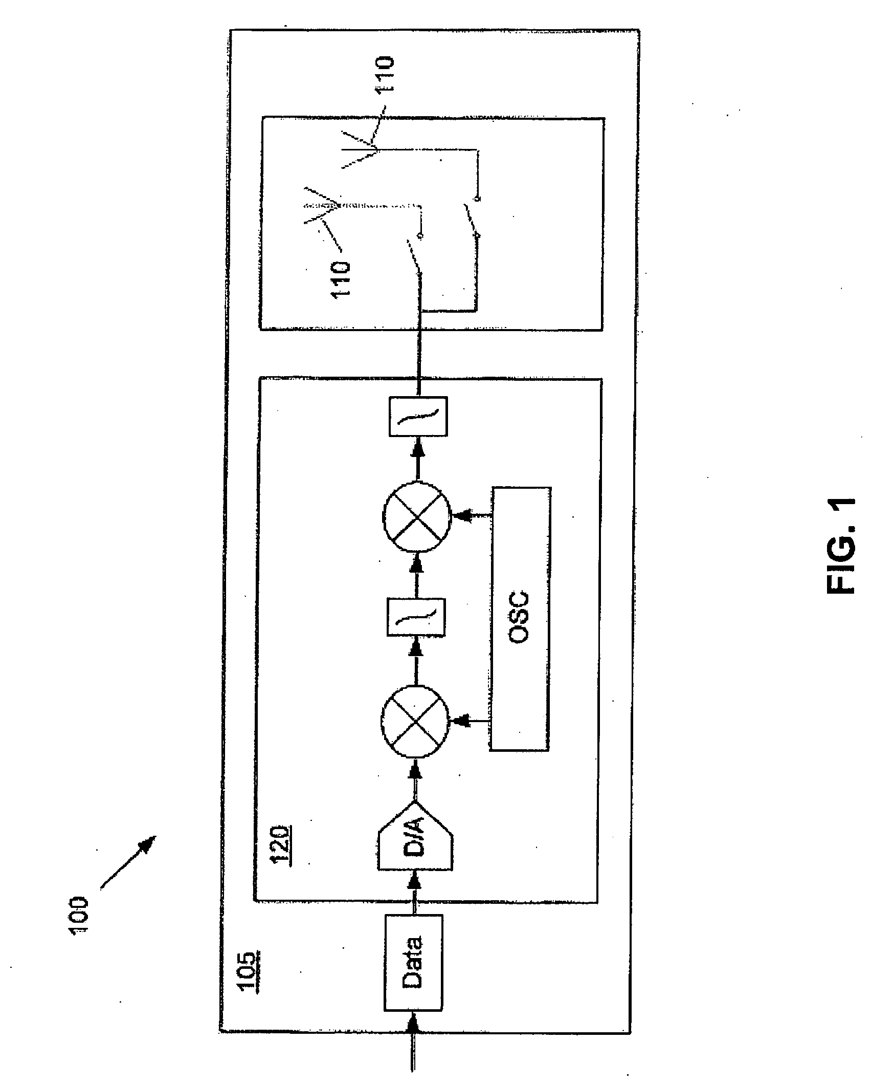
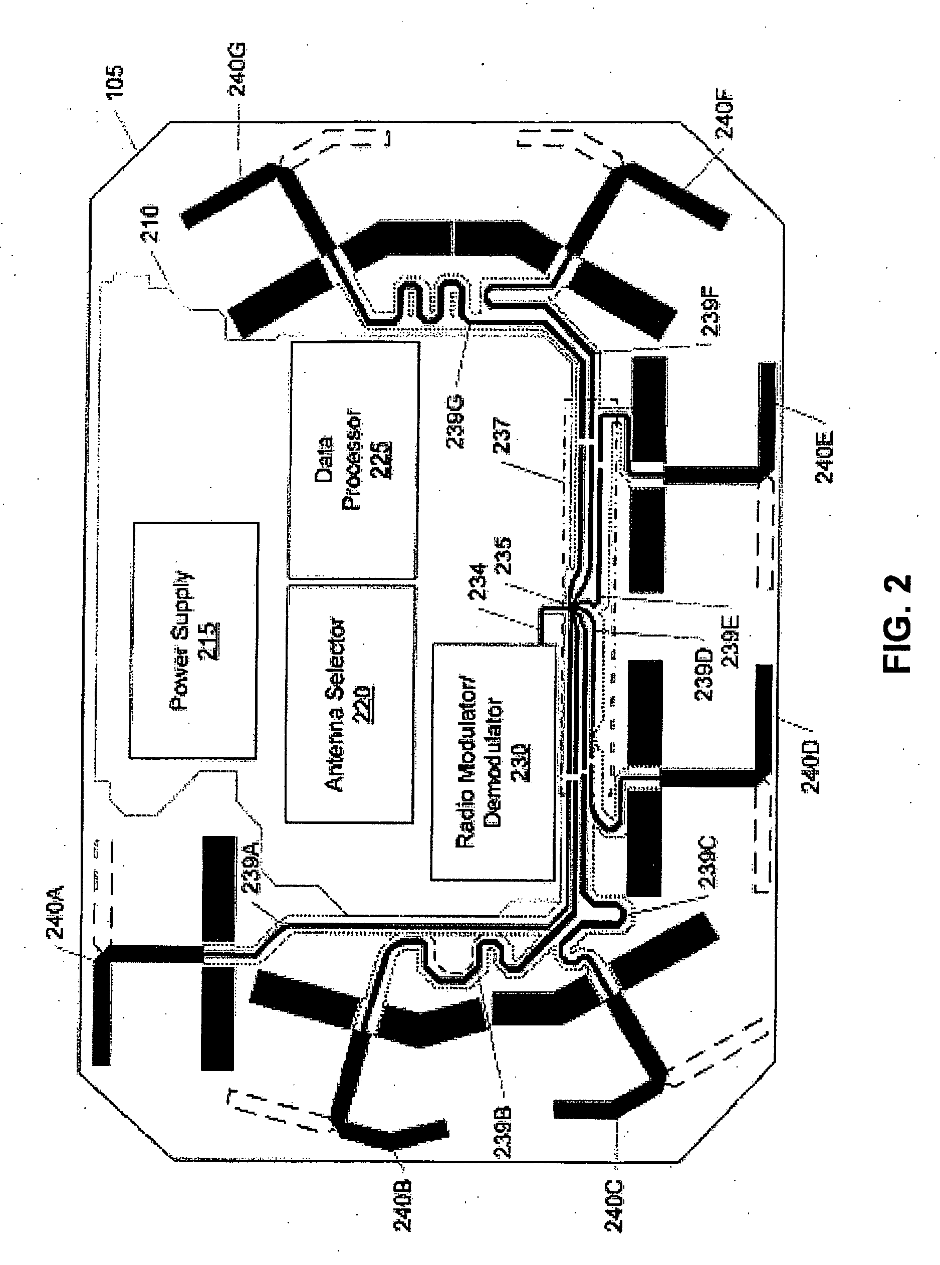
[0029] A system for a wireless (i.e., radio frequency or RF) link to a remote receiving device includes a circuit board comprising communication circuitry for generating an RF signal and an antenna apparatus for transmitting and / or receiving the RF signal. The antenna apparatus includes two or more antenna elements arranged near the periphery of the circuit board. Each of the antenna elements provides a directional radiation pattern. In some embodiments, the antenna elements may be electrically selected (e.g., switched on or off) so that the antenna apparatus may form configurable radiation patterns. If multiple antenna elements are switched on, the antenna apparatus may form an omnidirectional radiation pattern.

[0030] Advantageously, the circuit board interconnects the communication circuitry and provides the antenna apparatus in one easily manufacturable printed circuit board. Including the antenna apparatus in the printed circuit board reduces the cost to manufacture the unit an...


PUM


Abstract

A circuit board for wireless communications includes communication circuitry for modulating and/or demodulating a radio frequency (RF) signal and an antenna apparatus for transmitting and receiving the RF signal, the antenna apparatus having selectable antenna elements located near one or more peripheries of the circuit board and selectable phase shifting. A switching network couples one or more of the selectable elements to the communication circuitry and provides impedance matching regardless of which or how many of the antenna elements are selected, and includes a selectable phase shifter to allow the phase of the antenna elements to be shifted by 180 degrees. The phase shifter includes a first RF switch and two ¼-wavelength delay lines of PCB traces or delay elements and a second RF switch. The phase shifter selectively provides a straight-through path, a 180 degree phase shift, a high impedance state, or a notch filter.

Description

CROSS-REFERENCE TO RELATED APPLICATIONS [0001] This application is a continuation-in-part of U.S. patent application Ser. No. 11 / 022,080, filed Dec. 23, 2004, entitled “Circuit Board Having a Peripheral Antenna Apparatus with Selectable Antenna Elements,” which claims the benefit of U.S. Provisional Application No. 60 / 630,499, entitled “Method and Apparatus for Providing 360 Degree Coverage via Multiple Antenna Elements Co-located with Electronic Circuitry on a Printed Circuit Board Assembly,” filed Nov. 22, 2004, which are hereby incorporated by reference. This application is also related to co-pending U.S. patent application Ser. No. 11 / 010,076, entitled “System and Method for an Omnidirectional Planar Antenna Apparatus with Selectable Elements,” filed Dec. 9, 2004, which is hereby incorporated by reference.BACKGROUND OF INVENTION [0002] 1. Field of the Invention [0003] The present invention relates generally to wireless communications, and more particularly to a circuit board hav...

Claims


Application Information

Patent Timeline
Patent Type & Authority Applications(United States)
IPC IPC(8): H01P1/18
CPCH01P1/185
Inventor SHTROM, VICTOR
Owner ARRIS ENTERPRISES LLC
Why Eureka
Try Eureka