Semiconductor device and method of manufacturing the same

a technology of semiconductors and semiconductors, applied in the direction of semiconductor/solid-state device details, coupling device connections, instruments, etc., can solve the problems of difficult to increase the number of data lines, memory slots b>108/b> may also be damaged

Inactive Publication Date: 2006-06-08
SAMSUNG ELECTRONICS CO LTD
View PDF11 Cites 78 Cited by
  • Summary
  • Abstract
  • Description
  • Claims
  • Application Information

AI Technical Summary

Problems solved by technology

Further, the memory slot 108 may also be damaged.
Further, while increasing a number of data lines may decrease the latency for a memory device (e.g., memory car...

Method used


Image

  • Semiconductor device and method of manufacturing the same
  • Semiconductor device and method of manufacturing the same
  • Semiconductor device and method of manufacturing the same

Examples


Embodiment Construction

[0036] Hereinafter, example embodiments of the present invention will be described in detail with reference to the accompanying drawings.

[0037] In the Figures, the same reference numerals are used to denote the same elements throughout the drawings.

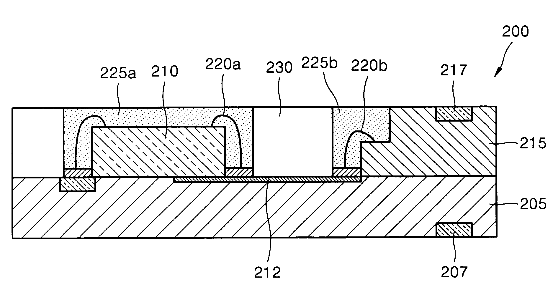
[0038]FIG. 6(a) illustrates a front contact pin array 217 of a memory card 200 according to an example embodiment of the present invention.

[0039]FIG. 6(b) illustrates a rear contact pin array 207 of the memory card 200 according to another example embodiment of the present invention.

[0040] In the example embodiment of FIG. 6(a), the front surface of the memory card 200 may include the front contact pin array 217 with first contact pins 1 through 9. In the example embodiment of FIG. 6(b), the rear surface of the memory card 200 may include the rear contact pin array 207 with second contact pins 1 through 9. In the front contact pin array 217, the first contact pins may be arranged with the first contact pin 9 located on a first side (e...


PUM


Abstract

A semiconductor device and method of fabricating the same. The semiconductor device includes at least one first contact pin on a first substrate and at least one second contact pin on a second substrate. The at least one first and second contact pins may be included in first and second contact pin arrays. The first and second contact pins of the first and second contact pin arrays may be aligned.

Description

PRIORITY STATEMENT [0001] This application claims the benefit of Korean Patent Application No. 10-2004-0103095, filed on Dec. 8, 2004, in the Korean Intellectual Property Office, the disclosure of which is incorporated herein in its entirety by reference. BACKGROUND OF THE INVENTION [0002] 1. Field of the Invention [0003] The present invention relates to a semiconductor device and a method of manufacturing the same, and more particularly, to a semiconductor device including contact pins and a method of manufacturing the same. [0004] 2. Description of the Related Art [0005] Memory cards may be widely used in electronic devices (e.g., multimedia devices, such as digital cameras and MP3 players). A memory card may include a given surface with a contact pin array for providing an electrical connection (e.g., with an associated electronic device). Accordingly, a user of the memory card may need to align the memory card in a proper orientation the memory card into a device's memory slot. ...

Claims


Application Information

Patent Timeline
IPC IPC(8): G06K19/06
CPCG06K19/07732G06K19/07743H05K1/117H05K1/141H05K2201/043H05K2201/09845H05K2201/10977H05K2203/049H01L2224/45144H01L2924/00H01L2224/45147H01L2224/48227H01L2924/19107H01L2924/181H01L2924/00014H01L2924/00012H01L23/28H01R12/71H01L21/60
Inventor HWANG, YI-SUNGCHO, SUNG-DAE
Owner SAMSUNG ELECTRONICS CO LTD
Why Eureka
Try Eureka