Electrical conductors in an electroluminescent display device

a technology of electroluminescent display device and electrical conductor, which is applied in the direction of electroluminescent light source, electric lighting source, solid-state device, etc., can solve the problems of increasing the difficulty of using ito for an electrode, and affecting the operation of the device. , to achieve the effect of large screen siz

Active Publication Date: 2006-06-15
SAMSUNG DISPLAY CO LTD
View PDF12 Cites 5 Cited by
  • Summary
  • Abstract
  • Description
  • Claims
  • Application Information

AI Technical Summary

Benefits of technology

[0013] It is therefore an object of the present invention to provide an improved design of an electroluminescent display device having a large screen size.

Problems solved by technology

Meanwhile, the above-described conventional electroluminescent display devices undergo a significant voltage drop due to a long distance from a cathode power supply source to some of the pixels in a large display.
Such a voltage drop becomes more problematic in front emission type electroluminescent display devices which has an high opening ratio.
However, use of ITO for an electrode can become problematic in electroluminescent display devices having a large screen size because ITO has a high enough resistivity to cause a voltage IR drop, especially for large screen sizes.
When such a voltage drop occurs, some pixels receive less voltage than other pixels, leading to non-uniform luminance distribution across the display.
However, an ITO or IZO layer thus formed at a low temperature has poor film quality and resistivity, and thus, a voltage drop phenomenon becomes significant.
Consequently, there arises a problem such as non-uniform luminance distribution of images displayed in electroluminescent display devices, particularly when the screen size is very large.
Also, pixels created by light emission from a light-emitting layer undergo color interference, by which creating high-definition images is difficult.
This voltage drop on the electrode can be problematic because it causes a non-uniform luminance distribution across the large screen of the display.

Method used


Image

  • Electrical conductors in an electroluminescent display device
  • Electrical conductors in an electroluminescent display device
  • Electrical conductors in an electroluminescent display device

Examples


first embodiment

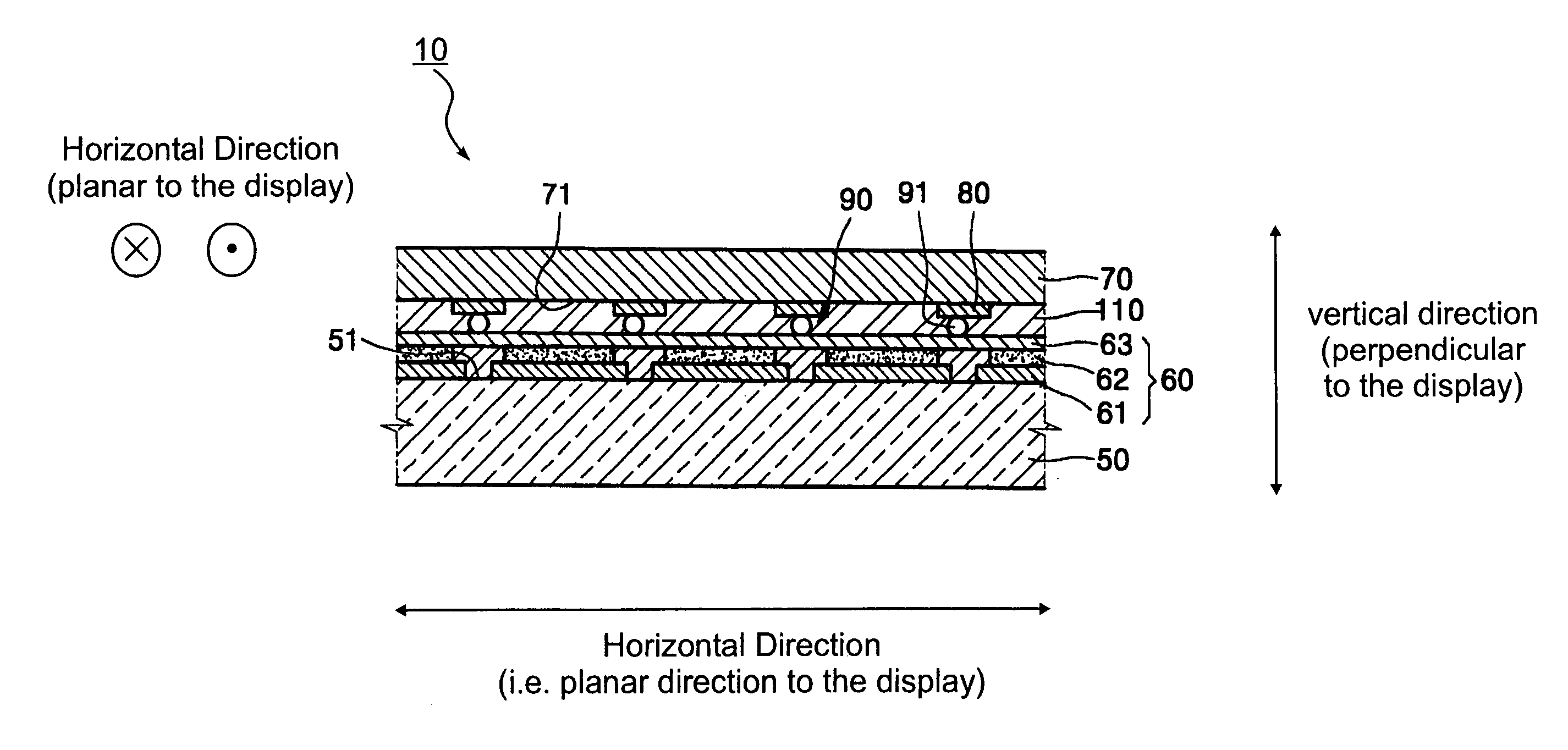
[0037] Turning now to the figures, FIG. 1 illustrates an electroluminescent display device 10 according to the present invention. Display device 10 is a passive device with a front emitting structure and is made up of a rear substrate 50 and a front substrate 70 that are coupled with each other. On an upper surface 51 of the rear substrate 50, a first electrode layer 61, a light-emitting layer 62, and a second electrode layer 63 are orderly formed. The first electrode layer 61, the light-emitting layer 62, and the second electrode layer 63 constitute a light-emitting unit 60. On a lower surface 71 of the front substrate 70, a conductive black matrix layer 80 is formed in a predetermined pattern to face the second electrode layer 63. The term, “predetermined pattern” as used herein indicates a pattern designed for inhibiting the passage of as little light as possible emitted from the light-emitting layer 62 toward the front substrate 70. The term “predetermined pattern” also infers t...

third embodiment

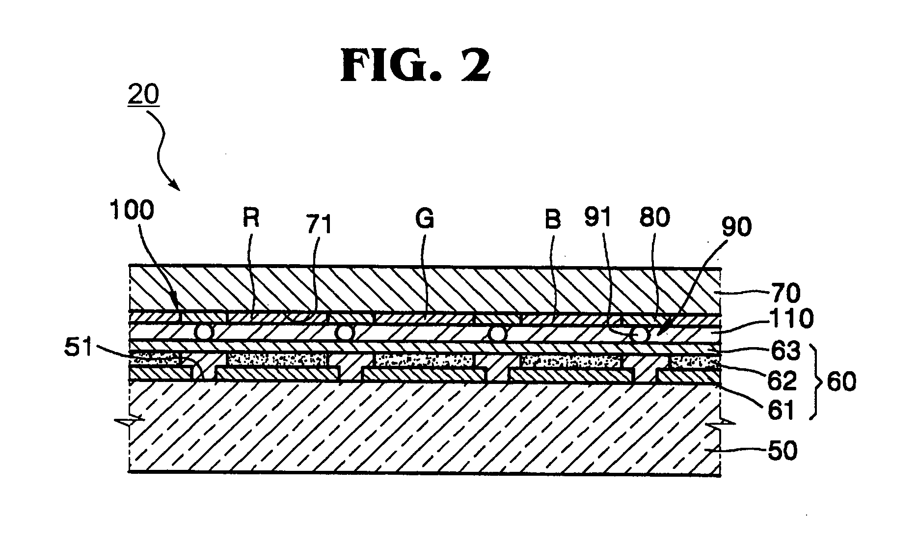
[0046] Referring to FIG. 3, the conductive protrusions 92 are formed on the black matrix layer 80 that is formed on the lower surface 71 of the front substrate 70 corresponding to regions between pixels of the light-emitting unit 60. The protrusions 92 may be made of conductive particles that are adhered to the black matrix layer 80 by a conductive paste. Color filter layers R, G, and B may be formed on the remaining lower surface 71 of the front substrate 70, on the same level as the patterned black matrix layer 80 between patterned portions of the black matrix layer 80. Preferably, a transparent and non-conducting filler 110 is interposed between each of the R, G and B color filter layers and the light-emitting unit 60. Non-conductive filer 110 is also disposed between adjacent conductive protrusions 92 in this third embodiment of the present invention.

[0047] An electroluminescent display device 200 according to a fourth embodiment of the present invention will now be described wi...

fourth embodiment

[0049] On a lower surface 271 of the front substrate 202, a black matrix layer 230 is formed. A plurality of connecting members such as conductive spacers 240 are interposed between the black matrix layer 230 and the transparent second electrode layer 211 to electrically connect black matrix layer 230 to each second electrode layer 211. Since only the second electrode layer 211 and not the black matrix layer 230 is made of a relatively highly resistive transparent conductive material, the voltage drop between the power supply or voltage source and each second electrode layer 211 in a display is low. Also, the potential at each second electrode layer 211 across the entire display is more uniform because there is little voltage drop across the black matrix layer 230. As in the first three embodiments, the fourth embodiment uses black matrix layer 230 and conductive spacers 240 to deliver power and voltage to the transparent second electrode layer 211 instead of using only transparent ...


PUM


Abstract

Provided is an electroluminescent display device having a negligibly small voltage drop of a cathode, no external light reflection, and high contrast and luminance. The electroluminescent display device includes a rear substrate, a first electrode layer formed above the rear substrate, a second electrode layer formed above the first electrode layer, the second electrode layer facing the first electrode layer, a light-emitting layer interposed between the first electrode layer and the second electrode layer, the light-emitting layer having at least an emission layer, a front substrate facing the rear substrate and contacting an upper surface of the second electrode layer, and a functional thin film formed between the second electrode layer and the front substrate, the functional thin film having a conductive material at least in a portion thereof contacting the second electrode layer.

Description

CLAIM OF PRIORITY [0001] This application claims priority to an application entitled “ELECTROLUMINESCENT DISPLAY DEVICE”, filed in the Korean Intellectual Priority Office on 13 Mar. 2003 and assigned Serial No. 2003-15686, and filed on 1 May 2003 and assigned Serial No. 2003-27991, the contents of that are hereby incorporated by reference. BACKGROUND OF THE INVENTION [0002] 1. Field of the Invention [0003] The present invention relates to an electroluminescent display device, and more particularly, to a design for conductors in an electroluminescent display device that reduces a voltage drop in an electrode layer on the light emitting side of an electroluminescent display device having a large screen size. [0004] 2. Description of the Related Art [0005] Since electroluminescent display devices have superior viewing angle, contrast, response time, weight, size, thickness, and power consumption compared to cathode ray tubes (CRTs) and liquid crystal displays (LCDs), much attention has...

Claims


Application Information

Patent Timeline
Patent Type & Authority Applications(United States)
IPC IPC(8): H01L33/00H01L29/22H01L29/227H05B33/26H01L27/12H01L27/32H01L51/50H01L51/52H05B33/14
CPCH01L27/12H01L27/322H01L27/3244H01L27/3246H01L27/3276H01L27/124H01L51/5221H01L51/5228H01L51/5237H01L51/5284H01L51/5206H10K59/38H10K59/122H10K59/12H10K59/131H10K50/814H10K50/82H10K50/824H10K50/8428H10K50/865
Inventor PARK, JIN-WOOKOO, JAE-BONLEE, KWAN-HEE
Owner SAMSUNG DISPLAY CO LTD
Why Eureka
Try Eureka