Semiconductor light emitting device and method for manufacturing the same

a technology of semiconductors and light emitters, which is applied in the direction of semiconductor devices, basic electric elements, electrical equipment, etc., can solve the problems of difficult to obtain satisfactory electrode characteristics, insufficient heat treatment, and electrodes provided on the semiconductor stacking structure, etc., to achieve high density, high density, and high accuracy

Active Publication Date: 2006-06-15
NICHIA CORP
View PDF8 Cites 92 Cited by
  • Summary
  • Abstract
  • Description
  • Claims
  • Application Information

AI Technical Summary

Benefits of technology

[0032] The present invention utilizes a part of the electrode provided on the semiconductor stacking structure as the electrode for external connection, thereby to achieve a device structure that has high density electrode structure, and various electrode structures and semiconductor stacking structures that can be formed with high accuracy so as to provide various light emitting devices in accordance to the application.
[0033] In the case of the light emitting device comprising the semiconductor stacking structure bonded onto the support member, the first and second electrodes of the semiconductor stacking structure can be disposed with high density and high accuracy on the bonding surface, and the light emitting device having high bonding accuracy can be manufactured, thus achieving a high yield of production even for the light emitting device of complicated structure.

Problems solved by technology

However, the structure of the light emitting device of the prior art does not allow it to extract sufficient light, and the electrodes of the light emitting device bonded onto the support member cannot be formed so as have sufficient characteristics suitable for a light emitting device due to constraints of the manufacturing process.
However, the electrodes provided on the semiconductor stacking structure after bonding it onto the support member can not be sufficiently heat treated due to restriction resulted from heat resistance of the bonding member.
As a result, it has been difficult to obtain satisfactory characteristics of the electrodes that are provided on the semiconductor stacking structure after bonding it onto the support member.
There is also such a problem that the structure and the arrangement of the electrodes in the semiconductor stacking structure are such that shade the emitted light depending on the material of the electrodes, and therefore the electrode structure involves advanced design.
For example, when the surface area of the light emitting device becomes larger, a part of the light emitting structure section may not emit sufficient amount of light due to the structure of the electrode even when the light emitting structure section has a surface area that is proportional to the surface area of the device.
Moreover, the light emitting structure section may instead absorb the light propagating in the light emitting device thus making it impossible to increase the optical output in proportion to the increase in the device area.
When the area of light emitting devices, area of the light emitting structure and the number of light emitting structure sections are increased, there arise such problems as the uniformity of light emission and loss of light in a portion having low efficiency of light emission.

Method used


Image

  • Semiconductor light emitting device and method for manufacturing the same
  • Semiconductor light emitting device and method for manufacturing the same
  • Semiconductor light emitting device and method for manufacturing the same

Examples


example 1

[0111] In Example 1, the semiconductor stacking structure 10 is constituted by forming n-type layer and p-type layer from nitride semiconductor on the semiconductor growing substrate 1, and forming the electrode forming section 11 (the exposed portion of the surface of the n-type layer 2) for forming the first electrode (n electrode) (FIG. 13A). The semiconductor stacking structure described above is employed for the specific stacked structure. As shown in FIG. 13A, a plurality of device structure sections 13 are provided on the semiconductor stacking structure 10 formed on the semiconductor growing substrate 1, while the first electrode forming section 11 and the adjacent light emitting structure section 12 are provided on the device structure section 13. The electrode forming section 11 has a forming section 11a interposed by the light emitting structure section 12 and, as can be seen in FIG. 12, an outside exposure section 11b where electrodes 21x are connected and external conne...

example 2

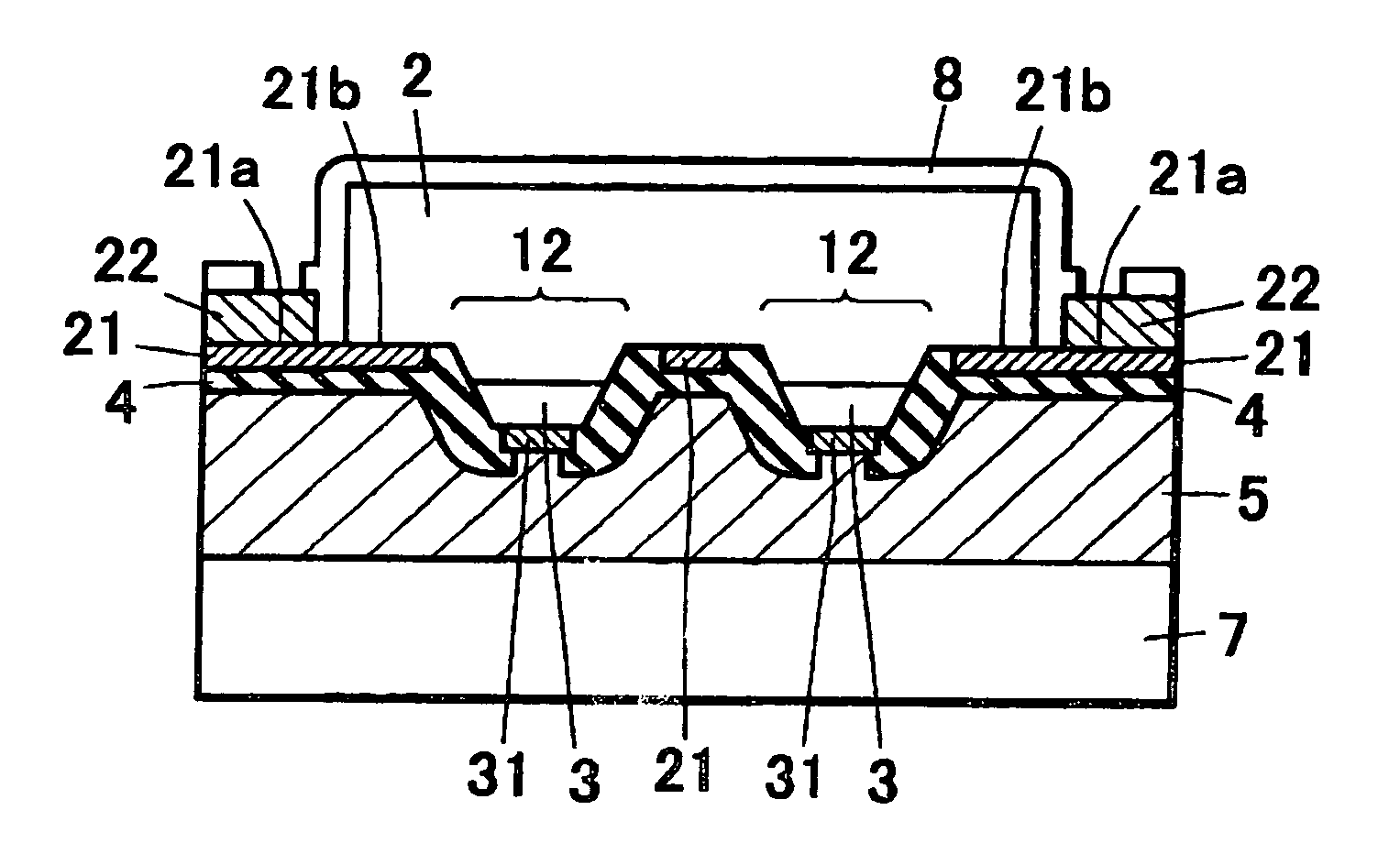
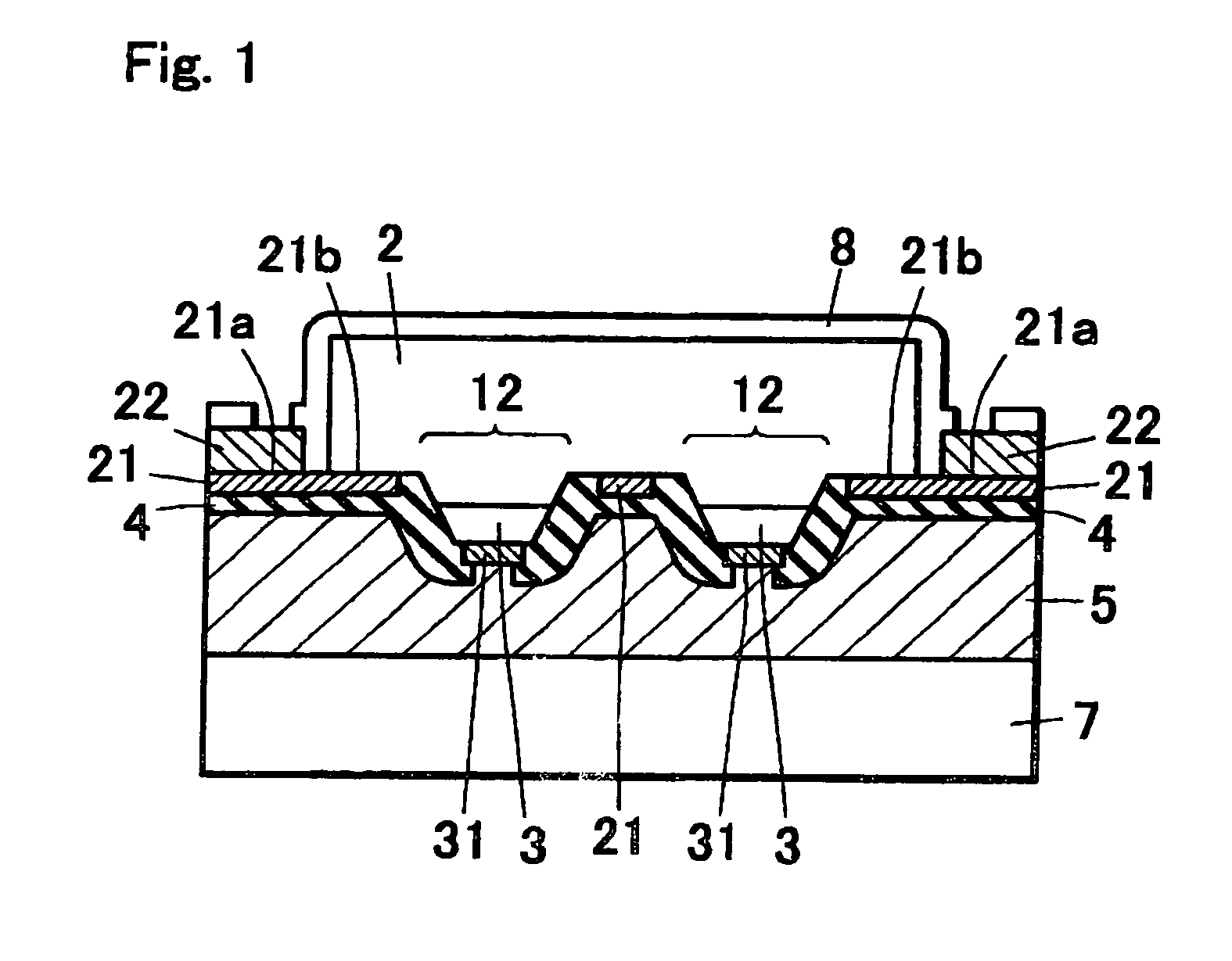
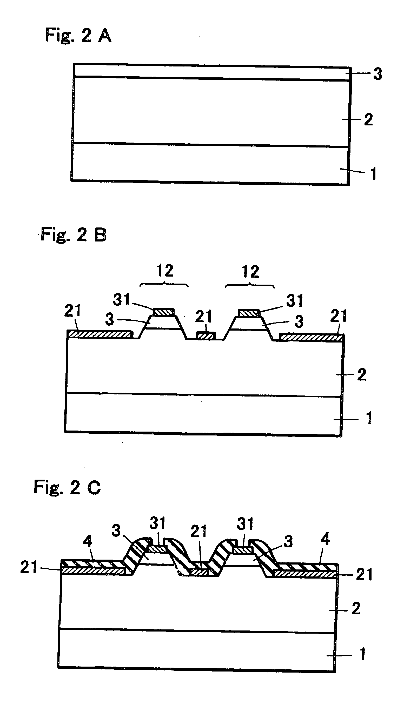
[0116] In Example 2, first the n-type layer 2 and the p-type layer 3 made of nitride semiconductor are grown on the semiconductor growing substrate 1 (FIG. 2A). Before growing the n-type layer 2 and the p-type layer 3, an underlying layer is grown but is not shown. Specifically, the stacked structure is constituted from the underlying layer (the low-temperature buffer layer, the first underlying layer, the second underlying layer), the n-type layer (the first n-type layer, the second n-type layer), the active layer and the p-type layer (the first through third p-type layers) laminated respectively on a sapphire substrate similarly to the semiconductor stacking structure shown above.

[0117] Then etching operation is carried out so as to expose the electrode forming surface (surface of the n-type layer 2) for the formation of the first electrode (n electrode) and separate into a plurality of light emitting structure sections 12, thereby to form the first electrode 21 on the electrode ...

example 3

[0126] In Example 3, a light emitting device that has the first electrode and the second electrode having the external connection section formed on the same surface with the semiconductor contact section is manufactured.

[0127] In Example 3, the n-type layer 2 and the p-type layer 3 are grown on the semiconductor growing substrate 1, etching operation is carried out so as to expose the electrode forming surface for the formation of the first electrode and separate into a plurality of light emitting structure sections 12, thereby to form the first electrode 21 on the electrode forming surface of the n-type layer 2, and form the second electrode 32 on the p-type layer 3 of the light emitting structure section 12 (FIG. 3A). In Example 3, the second electrode 32 is used as the common electrode for the plurality of light emitting structure sections, as shown in FIG. 3A.

[0128] Then the bonding member 5a for bonding with the support member 7 is applied between the first electrode 21 and t...


PUM


Abstract

A semiconductor light emitting device having a semiconductor stacking structure bonded onto the support member and having excellent characteristics is provided by a preferable electrode structure. The semiconductor light emitting device comprising; a semiconductor stacking structure having a first semiconductor layer and a second semiconductor layer of conductivity types different from each other, a first electrode connected to the first semiconductor layer, and a second electrode connected to the second semiconductor layer, wherein one principal surface of the first electrode has a portion that makes contact with the first semiconductor layer so as to establish electrical continuity and an external connection section.

Description

TECHNICAL FIELD [0001] The present invention relates a semiconductor light emitting device that has semiconductor stacking structure and, more particularly, to a semiconductor light emitting device that is bonded onto a support member, and a method for manufacturing the same. BACKGROUND ART [0002] A light emitting device based on a semiconductor is made by stacking semiconductor layers such as n-type and / or p-type so as to form a semiconductor stacking structure on a substrate and providing electrodes on the layers of different conductivity types, while electricity is supplied through the electrodes so that the device emits light. There is also such a light emitting device comprising a support member and a semiconductor stacking structure made by bonding a semiconductor device structure formed on a substrate onto the support member (for example, shown in FIG. 2 of Japanese Unexamined Patent Publication (Kokai) No. 2003-31858). [0003] However, the structure of the light emitting devi...

Claims


Application Information

Patent Timeline
Patent Type & Authority Applications(United States)
IPC IPC(8): H01L33/00H01L33/08H01L33/38
CPCH01L25/167H01L33/08H01L33/20H01L33/382H01L2224/48091H01L2224/48237H01L2224/49107H01L2924/00014H01L2924/01322H01L2924/12041H01L2224/73265H01L33/38
Inventor AKAISHI, KAZUYUKI
Owner NICHIA CORP
Why Eureka
Try Eureka