

Y/C separation with 3D comb filter
- Summary
- Abstract
- Description
- Claims
- Application Information
AI Technical Summary
Benefits of technology
Problems solved by technology
Method used
Image


Examples
Embodiment Construction
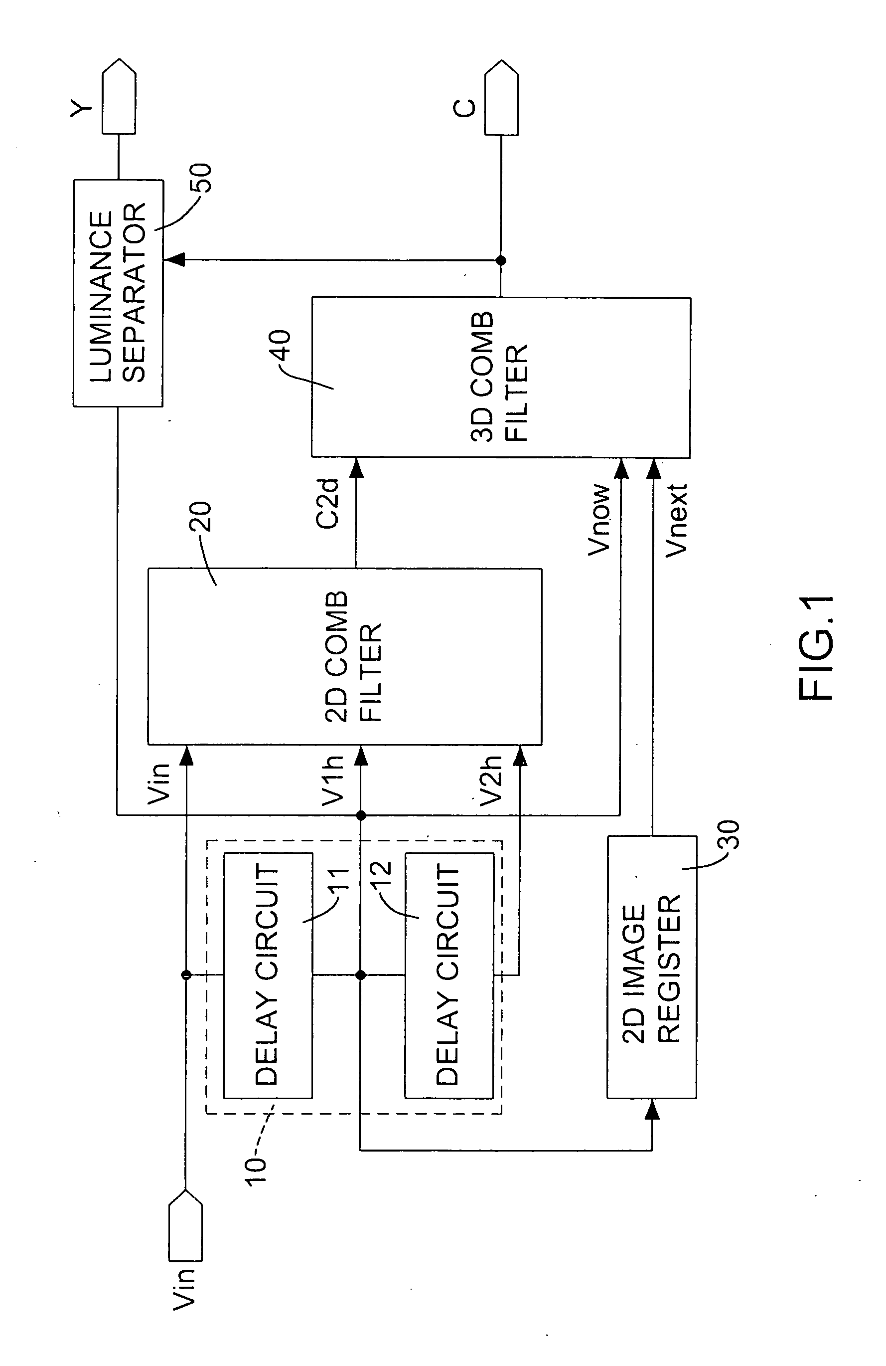
[0011] A Y / C separation circuit of a three-dimension (hereafter abbreviated as 3D) image signal of the present invention is provided. With reference to FIG. 1, a functional block diagram of the present invention includes a delay unit 10, a 2D comb filter 20, a 2D image register 30, a 3D comb filter 40 and a luminance separator 50.
[0012] The delay unit 10 includes two delay circuits 11 and 12. The two delay circuits 11, 12 are series connected to an image signal input terminal Vin for simultaneous outputting of a current image scan signal Vin and two scan signals V1h and V2h, which occur before and after the current scan signal Vin, respectively, so as to have three scan signals. Between the two delay circuits 11, 12 is the image scan signal V1h, which will undergo chrominance separation.
[0013] Every input terminal of the 2D comb filter 20 is connected respectively to the image signal input terminal and output terminals of the delay unit 10 to receive the three adjacent scan signal...
PUM
 Abstract
Description
Claims
Application Information