
Thin film transistor for imaging system

a technology imaging systems, applied in the field of thin film transistors for use in detectors, can solve the problems of poor image quality, two major noise sources associated with data lines, and other low-energy imaging techniques, and achieve the effect of reducing electronic nois

Inactive Publication Date: 2006-06-22
GENERAL ELECTRIC CO
View PDF5 Cites 10 Cited by
  • Summary
  • Abstract
  • Description
  • Claims
  • Application Information

AI Technical Summary

Benefits of technology

[0006] Therefore, there is a need for reducing the electronic noise generated by electronic components in the detector.

Problems solved by technology

However fluoroscopic techniques, as well as other low energy imaging techniques, may suffer from poor image quality due to the relatively weak X-ray signal relative to the electronic noise attributable to the detector.
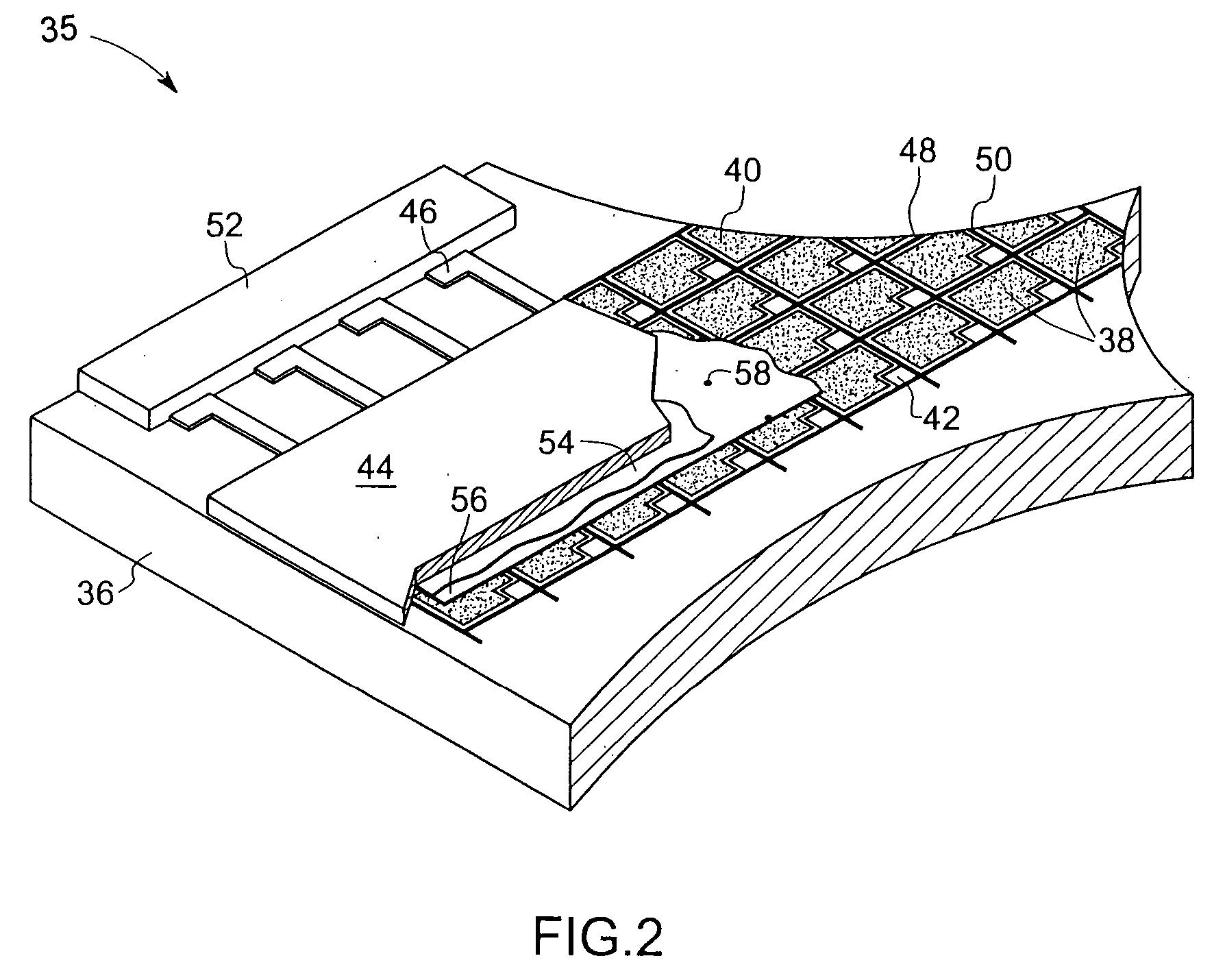
Various aspects of the thin film transistors (TFTs) employed in the detector may contribute to the overall electronic noise.
This in turn, leads to two major noise sources associated with the data line, namely the Johnson noise associated with the resistance of the data line and the noise associated with the read out electronics.
Further, the charge trapping currents in TFTs also contribute to the overall electronic noise.

Method used


Image

  • Thin film transistor for imaging system
  • Thin film transistor for imaging system
  • Thin film transistor for imaging system

Examples


Embodiment Construction

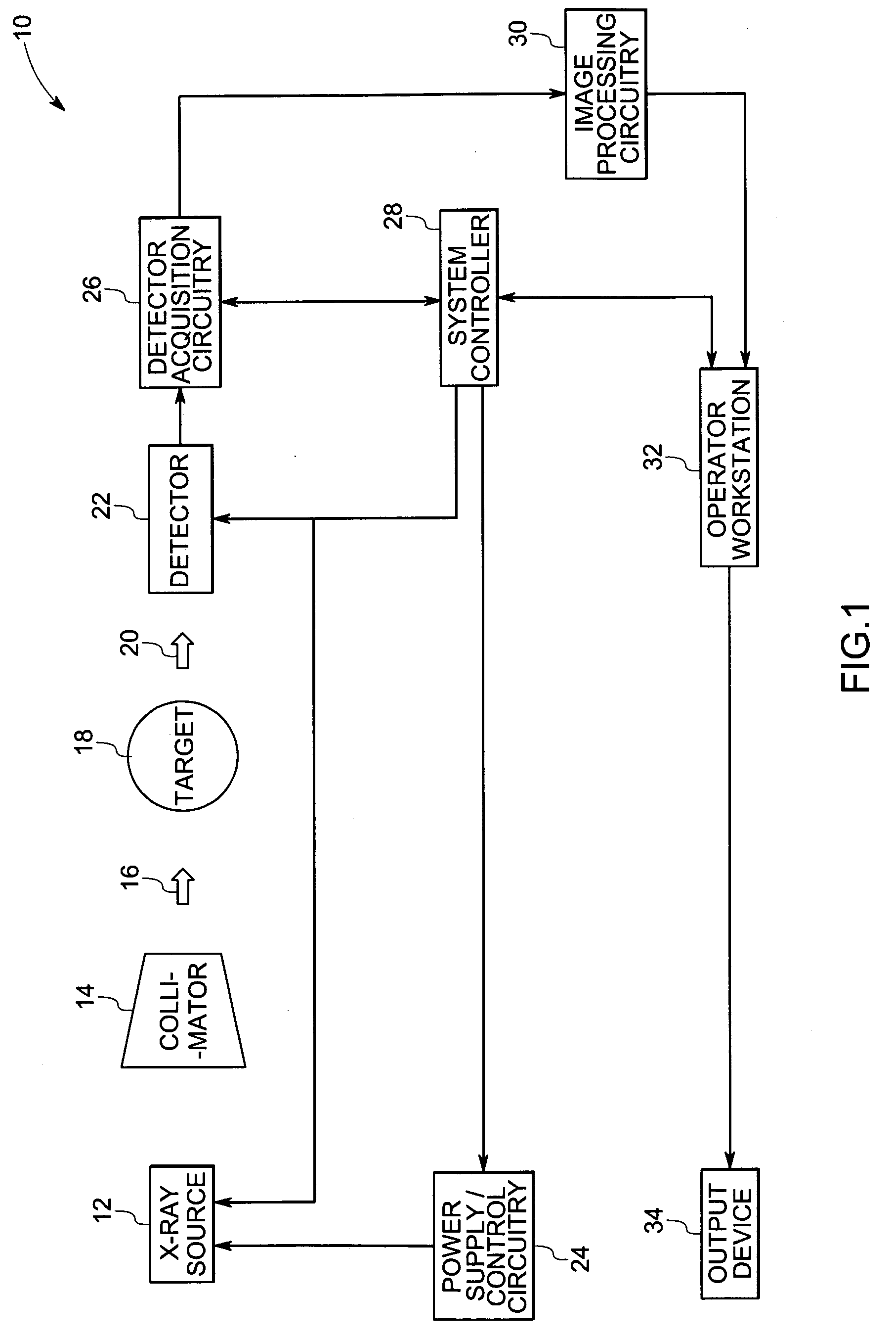
[0020]FIG. 1 is an illustration of an X-ray imaging system designated generally by a reference numeral 10. In the illustrated embodiment, the X-ray imaging system 10 is designed to acquire and process image data in accordance with the present technique, as will be described in greater detail below. The X-ray imaging system 10 includes an X-ray source 12 positioned adjacent to a collimator 14. In one embodiment, the X-ray source 12 is a low-energy source and is employed in low energy imaging techniques, such as fluoroscopic techniques, or the like. Collimator 14 permits a stream of X-ray radiation 16 to pass into a region in which a target 18, such as a human patient, is positioned. A portion of the radiation is attenuated by the target 18. This attenuated radiation 20 impacts a detector 22, such as a fluoroscopic detector. As will be appreciated by one of ordinary skill in the art, the detector 22 may be based on scintillation, i.e., optical conversion, on direct conversion, or on o...


PUM


Abstract

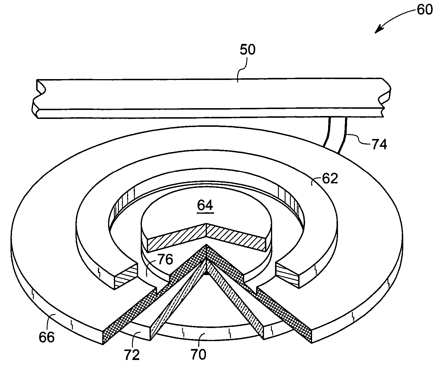
An annular thin film transistor includes an annular source electrode disposed above the layer of the semiconductor material, a drain electrode disposed above the layer of the semiconductor material within the annular source electrode, and an active channel between the drain electrode and the annular source electrode, wherein a surface of the active channel comprises exposed semiconductor material. Further, a serpentine thin film transistor includes a serpentine source electrode disposed above the layer of the semiconductor material, a drain electrode disposed above the layer of semiconductor material and substantially within a recess formed by the serpentine source electrode, wherein the drain electrode is configured to substantially conform to the recess, and an active channel between the drain electrode and the serpentine source electrode, wherein the active channel has a substantially consistent length, and wherein a surface of the active channel comprises exposed semiconductor material.

Description

BACKGROUND [0001] The invention relates generally to imaging systems. In particular, the invention relates to thin film transistors for use in detectors of such imaging systems. [0002] Non-invasive imaging broadly encompasses techniques for generating images of the internal structures or regions of a person or object that are otherwise inaccessible for visual inspection. For example, non-invasive imaging techniques are commonly used in the industrial field for inspecting the internal structures of parts and in the security field for inspecting the contents of packages, clothing, and so forth. One of the best known uses of non-invasive imaging, however, is in the medical arts where these techniques are used to generate images of organs and / or bones inside a patient which would otherwise not be visible. [0003] One class of non-invasive imaging techniques that may be used in these various fields is based on the differential transmission of X-rays through a patient or object. In the med...

Claims


Application Information

Patent Timeline
Patent Type & Authority Applications(United States)
IPC IPC(8): H01L31/062
CPCH01L27/12H01L27/14658H01L29/41733H01L29/78618
Inventor ALBAGLI, DOUGLASHENNESSY, WILLIAM ANDREWCOUTURE, AARON JUDYCOLLAZO-DAVILA, CHRISTOPHER
Owner GENERAL ELECTRIC CO
Learn More